


SUMIT provides a very flexible combination of high-speed serial buses and legacy I/O support for enabling powerful embedded I/O module designs in small form factors.
This article examines the technical approaches and benefits to designing with the new SUMIT specification for embedded I/O modules. In addition, the concept of lane shifting will be explored in depth as it pertains to PCI Express lanes as well as USB. Ampro by ADLINK’s MiniModule SIO is then described as an example of a state-of-the-art real-world product design of such a SUMIT module.
Introduction to SUMIT
SUMIT is a stackable expansion connector specification targeted for new products. It includes both state-of-the-art serial buses and legacy chipset expansion buses, all in the same form factor. The specification is an I/O-centric approach that defines the connector and stacking method, but is independent of the stacked board form factors. SUMIT combines past and future expansion approaches in one very versatile specification. Figure 1 shows the basic structure of the SUMIT specification and summarises the buses, interfaces and signals carried.
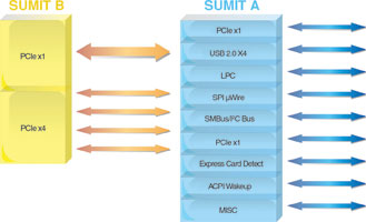
Two connectors are used on each expansion module - SUMIT A and SUMIT B. These connectors carry multiple high-speed serial PCIe and USB 2.0 buses for current and future applications, as well as including LPC, SPI and SMBus/I²C for legacy requirements.
The SUMIT B connector carries mostly PCIe interfaces, while the SUMIT A connector carries a single x1 PCIe and four USB 2.0 buses, as well as the legacy interfaces. Each SUMIT module generally has an upper and lower SUMIT A, and an upper and lower SUMIT B. For some lower-cost modules, only SUMIT A is needed and this is allowed for in the specification; SUMIT B is optional but is usually used in most module implementations.
The alignment and separation of the two SUMIT A and SUMIT B connectors is defined in the SUMIT specification, but the size of the module is not defined and can vary. This flexibility allows boards that follow the SUMIT specification to be connected together easily, even if their form factors differ.
SUMIT uses two connectors that are high-speed, fine-pitch (0,635 mm) stacking connectors with a central ground blade which gives good impedance control for the transfer of the high-speed serial buses between modules. Different stacking heights are available for the connector, for use where the expansion modules require additional clearance between modules for bulky components on the module; the standard stack heights currently are 15,24 mm and 22 mm.
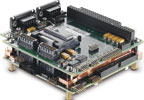
A stacked SUMIT system is shown in Figure 2. This example consists of a lower module board that is an Ampro CoreModule 730 and an upper module board that is an Ampro MiniModule SIO. The two SUMIT connectors can be seen on the top side of the top module on the board edge near to the camera. Note that the two boards have differing form factors in this case, and the connectors are relatively small and compact even though they transfer many high-speed buses between these two modules.
PCIe implementation in SUMIT
As mentioned earlier, SUMIT carries multiple PCIe interfaces on both connectors. Specifically, connector SUMIT B has a x1 lane PCIe link, and a x4 lane PCIe link, which may be used together or as individual lanes. Connector SUMIT A has a single link x1 lane of PCIe.
One of the significant features of SUMIT is the link-shifting method used for these PCIe buses, which allows straightforward distribution of links to the modules in the stack. Link-shifting allows easy stacking of multiple boards, while avoiding configuration jumpers or switches to set up the PCIe routing. An important point is that the shift method allows good layout to be achieved on the module boards to pass high-speed signal buses from board to board, up the stack.
To aid understanding of the link-shifting method, Figure 3 illustrates the concept in a generic, simplified form for three stacked boards - X, Y and Z - with four links originating on the base board (X) of the stack. Each board uses one link internally from the four passed up from below, and then passes the remaining links up to the board above, but with a shift of all these remaining links to the left. This shift is to account for the link that is used internally and that is not transferred to the board above.
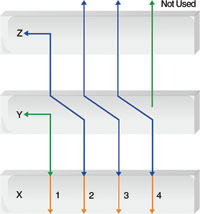
For example, board Y uses link 1 internally and passes up the three remaining links to board Z, which uses link 2 internally. However, board Z does not need to be reconfigured to take into account of the position of the board being above board Y, because board Z always gets the link it uses internally from the leftmost side of the set of links. This approach therefore allows easy stacking of multiple boards without needing any hardware configuration to indicate which links are to be used on particular boards.
Each module in the stack uses the links starting at the left side. Obviously the modules cannot use more links than are provided by the base module, but the distribution of links between modules occurs naturally as a result of the stacking with this shift method. A significant advantage of this approach is that the link-shift is done over small distances between connector pins, so an optimal PCB layout is possible, which is important in order to maintain signal integrity for the high-speed PCIe buses used.
Figure 4 shows the actual PCIe link-shifting method used in the SUMIT specification. Because the PCIe lanes are distributed over both connector SUMIT A and connector SUMIT B, the link-shifting also goes between these two connectors. The x1 link from SUMIT B gets shifted to SUMIT A, and the first link of the x4 gets shifted to the x1 link on connector B.
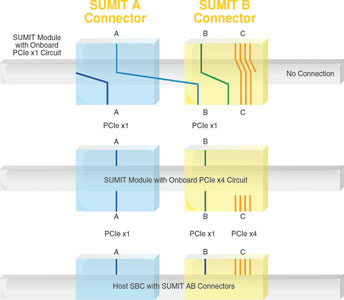
Note that a board that uses the x4 links on SUMIT B (but neither of the x1 links) should be the second board up in the stack and the x4 bus is not then transferred upwards. In that case the x1 links on SUMIT A and B are passed straight up through that board with no shift. If a link is not used internally in the board, a shift is not needed. When link-shifting occurs, the link clocks are shifted along with the data signals so as to ensure they stay matched together.
Support for other buses
SUMIT defines 4 USB 2.0 buses being available, for which bus shifting is also used. The USB buses are shifted between module connector A pins in a similar way to the PCIe link shifting. For example, if a module at the base of the stack uses the USB-0 bus on SUMIT A, it passes up the remaining three USB buses to any modules stacked above. This bus shift method allows the available USB buses to be simply distributed to the modules in the stack, without any extra module configuration being needed. The same benefit of a good PCB layout being achievable for the transfer of the USB buses from board to board, as in the PCIe case, applies here too.
The low-pin-count (LPC) bus is designed for attaching legacy peripherals, and is included in the SUMIT specification to allow a wide range of legacy interfaces to be used within the SUMIT stack of modules. LPC capabilities complement those available on the high-speed PCIe and USB interfaces, and this provides flexibility for implementing user applications, whilst still providing state-of-the-art high-speed buses on the SUMIT stack.
I²C and SPI are widely used medium-speed serial interfaces that are provided on the SUMIT connectors for connecting to devices on the module that use these buses. In particular, the SPI bus is becoming a more and more popular addition in many chipset designs.
MiniBlade is a new storage specification that uses USB and PCIe interfaces and naturally fits into the SUMIT implementation because of the availability of both interfaces on the connector stack. This storage form factor provides rugged capability to be able to withstand large amounts of shock and vibration.
MiniModule SIO example
For a real-world application example of SUMIT, Figure 5 shows the ADLINK MiniModule SIO module. This is an example of a versatile SUMIT module that illustrates an implementation of many of the features discussed earlier.
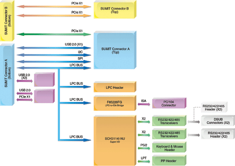
On the SUMIT A connector of this module there is a MiniBlade interface which uses one USB bus and one PCIe link. Two additional USB buses are also brought to a header for connecting USB to user application hardware external to the module. The remaining USB bus is not used on the module and so it is transferred to the upper module connector. So the next stacked board above the MiniModule SIO could use this USB 2.0 bus for the application. The MiniModule SIO is therefore a good example of an implementation of the USB bus shift method described in the SUMIT specification.
The MiniModule SIO uses the LPC to implement a whole set of legacy I/O interfaces, including a full ISA bus on PC/104 connectors. This uses the SUMIT LPC bus to interface to an LPC-to-ISA bridge. In this way SUMIT can easily support PC/104. An SMSC 3114 SIO is also included to provide rugged I/O capability in the design, and this chip provides the quad serial RS232/422/485 interfaces on dual DB connector interfaces, and on dual header interfaces, along with a keyboard and mouse interface and a legacy parallel port on a header.
Because this MiniModule SIO module uses up one PCIe link in the MiniBlade interface, the remaining PCIe Links are link-shifted. So SUMIT B x1 PCIe is transferred, through a link-shift, to SUMIT A x1. Although the x4 PCIe is not shown in this diagram, because of the link-shift of the x1 PCIe from SUMIT B to SUMIT A, the x4 PCI is also link-shifted within the SUMIT B. The SPI bus is not used in this module so it is simply transferred through this module from the lower board to the board above on the SUMIT A connectors.
| Tel: | +27 12 493 0852 |
| Email: | [email protected] |
| www: | www.epd.co.za |
| Articles: | More information and articles about Electronic Products Design |


© Technews Publishing (Pty) Ltd | All Rights Reserved
 printer friendly version