


Optimisation of cost and reduction of size are driving the need to integrate the components in current transducers using application-specific integrated circuits (ASICs).
The target of cost optimisation means that standard commodity silicon processes with no special manufacturing steps must be used. This leads to a paradox: how to use an ASIC made entirely of elements whose critical parameters vary by several hundred ppm/°C to make measurements with a precision of 1% to 2% over all operating conditions.
The target is made even more challenging when the need for a very fast response time is added. This article describes a new LEM ASIC which achieves this objective while at the same time adding extra functionality.
Technology and quality evolution
In many current measurement applications, it is advantageous that the measuring circuits are isolated from the measured current, and in these cases the magnetic field due to the current can be concentrated at a sensor to which it is sensitive. In an ASIC, a Hall cell may be used to transform the magnetic field into a voltage. A Hall cell, however, is not only a particularly unstable element, but additionally its properties are usually not guaranteed in an ASIC manufacturing process.
Current transducer architectures have been developed which are insensitive to the stability and linearity of the magnetic sensor, for example the closed-loop architecture shown in Figure 1a.
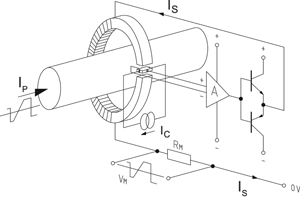
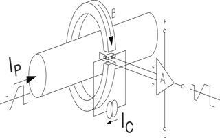
However, such an architecture is still sensitive to offsets in the sensor, and in any case the ultimate goal for cost and reliability is to develop an open-loop transducer containing no electrical components except the ASIC – see Figure 1b – while having the performance of a closed-loop architecture.
Fully integrated ASICs for open-loop current transducers such as LEM’s HXS series have been developed in the past.
The performance is satisfactory, with typical specification parameters as follows:
* Gain drift: 350 ppm/°C;
* Input related offset drift: 2 μT/°C;
* Response time: 5 μs;
* Output noise density: 7 μV/rtHz with a sensitivity of 40 V/T in a fixed bandwidth;
* Current consumption: about 15 mA.
These ‘first generation’ ASICs have a rigid architecture where only gain (sensitivity) is adjustable and is stored in a memory which can only be written once, which limits the flexibility of their use.
Advances in silicon manufacturing technology and also in quality standards give a serendipitous combination of process changes that permit the design of a ‘second generation’ family of ASICs. These advances are:
* Analog elements which are fast and dense;
* Digital elements which are dense enough to add useful functionality within a limited cost budget;
* EEPROM memory which can be rewritten as many times as needed;
* The three above features are available in processes such as the 180 nm and 350 nm nodes which are somewhat behind the state of the art, and so are at a reasonable cost;
* There is also an apparently unrelated development, which is that quality standards such as the automotive AEC-Q100 require testing at two or three temperatures.
Of course these factors are accompanied by some disadvantages. The need for both high speed and low noise increases power consumption. The best transistors are 3,3 V devices, but the market requires operation in a 5 V environment.
However, putting these developments together has allowed LEM to design an ASIC in which the company targeted at least a twofold improvement in the critical parameters of the first generation listed above. At the same time the company has been able to add features such as an over-current detection (OCD) output, and the final circuit configuration may be chosen at any time in the process, even by the end user of the current transducer using the ASIC.
The result is a cost-effective Hall-cell based ASIC with fast response time and low temperature drifts. Figure 2 shows a block diagram of the ASIC. To minimise the effect of offsets in the Hall cells, conventional spinning techniques are used with an output at 1,5 MHz and the eight cells are placed in an optimised symmetrical arrangement.
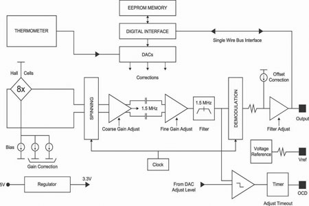
Using eight cells improves the signal-to-noise ratio of the signal at the input to the electrical chain to a level similar to that of dedicated Hall cells made with III-V compounds such as Gallium Arsenide, though the low signal level at this point means that the following amplifier has to have a low noise level. It is physically large and consumes a high current: about 8 mA for the Hall cell and amplifier combination.
The signal is amplified with high gain-bandwidth amplifiers and is filtered before demodulation to limit the noise which is folded back into baseband. The filter uses the same elements as the oscillator which sets the spinning frequency, and so can have quite a narrow bandwidth despite the process variations.
The OCD block input is taken before the demodulator and final output amplifier/filter which has two advantages: it accommodates signals outside the linear operating range of the output, and it has a fast response which is independent of the output filter bandwidth.
The latter may be chosen for the best compromise between the response time of the signal channel and the noise level at the output. A timer block at the OCD output allows a hold time of up to 1 ms, if needed, to ensure that a short overload may still be detected by an external microcontroller.
In order to meet a quality commitment at the ppm level, testing of the packaged ASIC is done at cold and/or hot before the final test at ambient temperature. This allows drifts of gain and offset to be measured and an opposite correction to be stored in EEPROM.
These data are combined with the output of an on-chip thermometer and digital-to-analog converters to generate analog corrections of the unavoidable gain and offset drifts in a standard silicon process. Indeed, several corrections may be stored for different ASIC configurations and correction automatically applied for the configuration chosen.
If the Vref pin of the ASIC is forced to the supply voltage, the output pin becomes the I/O port of a single-wire bus interface. This means that the final ASIC configuration may be decided at any time, even in the final application of the LEM current transducer.
For example, two users may both want to measure currents in the same range. For one a fast response time may be the most important parameter while the other prefers low output noise. Each may choose the output filter bandwidth by configuring the ASIC according to their preference.
The magnetic sensitivity may be chosen between 5 and 200 V/T with 0,5% precision by sharing the 12 bits of data between exponential steps of 15% in the coarse gain adjustment and 32 steps of 0,5% in the linear adjustment.
The real challenge in design is to improve all the critical parameters, since generally they impose opposite constraints. The measured specification parameters of the new LEM ASIC are given below:
* Gain drift: typical 100, maximum 200 ppm/°C;
* Input related offset drift: typical 0,3, maximum 1,0 uT/°C;
* Response time: < 2 μs;
* Output noise density: 6 μV/rtHz with a sensitivity of 40 V/T in a selectable bandwidth;
* Current consumption: 19 mA;
* Die area: slightly smaller than the first-generation equivalent.
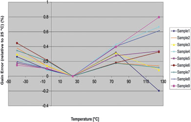
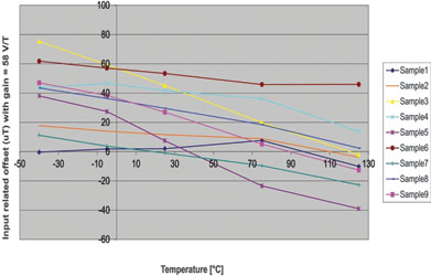
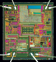
Measured parameters from LEM’s standard validation setup which checks nine circuits at a time are shown in Figures 3a and 3b. A die photograph is shown in Figure 4 – the eight Hall cells can be seen at the centre of the die.
Conclusion.
The new LEM ASIC described meets the target of improved precision for open-loop, Hall-effect based current transducers. Looking forward, the company believes that more improvements are possible, both by adding more features and by using new design techniques to achieve the same level of precision while reducing the calibrations needed.
| Tel: | +27 11 626 2023 |
| Email: | [email protected] |
| www: | www.denver-tech.co.za |
| Articles: | More information and articles about Denver Technical Products |


© Technews Publishing (Pty) Ltd | All Rights Reserved
 printer friendly version