


Some may think that digital circuits, especially using CMOS and BiCMOS, are easy to design. But like most things in life, professionals who have many years of experience make the jobs look easy. The circus performer effortlessly juggles many items. The concrete finisher creates a smooth surface, and a top chef creates a gourmet meal in a snap.
Now back to circuit design. Is digital design not just stringing together some logic gates? If only life were so simple. Proper power management, power decoupling and grounds are essential for a successful design.
In this article, we discuss CMOS and BiCMOS ICs and show how a simple mistake – no VCC – triggers odd behaviour. We will explain why that low-power CMOS device might be burning hot. Finally, we examine how that relates to circuit turn-on times.
Note that we are not talking about specific applications or parts. This topic is endemic to IC design and transcends any specific device usage. The focus here is on the details and how careful design will not waste anything – space, current, power, you name it – or burn your hand!
Why did I burn my finger on the IC?
One of the hallmarks of CMOS or BiCMOS is low power consumption. A CMOS gate only draws power on transitions, so those circuits run cool at slow speeds.
Fine, but why is the board hot?
Figure 1 shows a simple CMOS circuit. It is complementary (N and P devices – hence the name complementary metal oxide semiconductor). It is ones and zeros and so simple. At any given moment, one device is on, the other is off. What could possibly go wrong? It turns out there are some conditions that can cause the circuit to draw quite a lot of power.
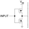
When the CMOS circuit is approximately midway between one and zero, both the top and bottom transistors are partially on. Consequently, the faster the speed, the more transitions per second and the more power used. As long as the transitions are fast, the part does not stay in the middle position long and everyone is happy. Table 1 shows some safe logic high and low levels as a percentage of power supply voltages.
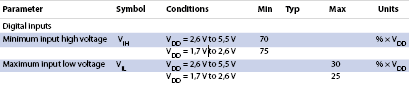
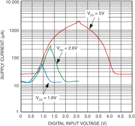
Logic levels are typically specified as a percentage of the power-supply voltage. The waveform of Figure 2 is made by slowly changing the input voltage. If the application is, regrettably, at 2,6 V with a 5 V supply, it will draw 80 times more current than with the proper one and zero. In the case of a 5 V logic swing, if the signal is less than 0,7 V, it is a safe zero; if it is above 4,3 V, it is a safe one.
The MAX5391 will interface 5 V logic with a 5 V supply and will accommodate 3 V logic with a 3 V supply. Now suppose that someone wants to mate this part to 3 V logic in the input, but with a 5 V supply? The zero case works, but the one draws four to eight times more power than necessary.
This is why the CMOS could be running hot. The proper fix is to use a logic-level translator between logic running at different voltages.
Other turn-offs or turn-ons
Generally humans enjoy people watching. Engineers, in particular, enjoy details, and what exactly are the turn-ons and turn-offs that matter so much?
The issue is really about power sequencing. IC designers would like the power supplied to all pins to be applied simultaneously or at least in a prescribed order. System engineers know that this is nearly impossible without extraordinary effort and numerous extra circuits.
Consequently, most circuits must fend for themselves and, at a minimum, not destroy themselves for the few seconds while the power supply stabilises.
Thankfully, modern parts are not like some early ICs that internally latched up and self-destructed if power was not applied in the prescribed order. Yet there are some circuits such as logic, ASICs or processors that must be powered before logic-levels signals are applied to their inputs. The system designer must understand why this is true, not theoretically but in reality.
Most system designers with a few years of experience have seen someone trying to troubleshoot a CMOS logic issue. The problem comes and goes, seemingly at random. Just when something starts to make sense, everything changes. The circuit nodes that were behaving properly suddenly are not.
Have you guessed the answer? Yes, of course! The CMOS was missing a power supply. A CMOS requires such a small amount of power that it will operate if one input pin is at a logic-high level. How does it work?
Picture a group of logic gates without VCC applied (Figure 3). Here the group has all the VCC pins tied together on a bus. Now apply a logic high from an external, properly powered circuit to the signal pin C.
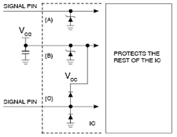
The high level goes through the top ESD diode to the VCC bus. Now all the gates have power and appear to work... until the logic high on pin C becomes a zero or low. That section of logic then stops working until any input pin goes high.
With several input pins like the above, the group appears to do silly, illogical things. This situation is not fun to troubleshoot and leads to a fundamental rule of design: always start with the basics – is it plugged in and is power and ground present at the proper voltages?
The ESD structures inside an IC are designed to protect the part before the customer mounts it on a product’s printed circuit board. The ESD diodes inside the ICs are limited in size; they cannot withstand system ESD events that come from external sources.
Powerline surges and close lightning strikes will overwhelm the internal IC ESD diodes. There are practical limits to fixing ESD, and external ESD parts are needed on printed circuit boards and systems.
Imagine a circuit that has a robust power source connected to pin C in Figure 3. VCC is off for a prolonged time. The top ESD diode will try to power everything on the VCC rail. However, the ESD diode is tiny and might fail over time. In that case, there may be a reason that VCC is removed, for example to reduce power consumption.
So adding an external diode in parallel with the top ESD diode solves the issue. The external diode (Si or Schottky) will carry the current and protect the IC.
Conclusion
The wisdom of experience hopefully allows us to design around some frustrating situations. If not, at least we can avoid some painful lessons. Attention to details is important. There are particular issues with the turn-on and turn-off times for CMOS and BiCMOS ICs, and thus we have explained how to estimate their turn-on times and calculate a CMOS circuit’s behaviour without VCC applied.
Finally, a CMOS/BiCMOS device can be running ‘burning’ hot if safe ones and zero levels are not maintained. The best fix is a logic-level translator running between the different voltages.
An old proverb says, ‘An ounce of prevention is worth a pound of cure.’ That is certainly true in circuit design. A good working knowledge of the digital logic family in a design is the best way to ensure that the resulting circuits are reliable, stay cool, and do not use any more current than necessary. That thought upfront can save a recall or revision or board spin later.
For more information contact Michelle Parreira, CST Electronics, +27 (0)11 608 0070, [email protected], www.cstelectronics.co.za
| Tel: | +27 11 608 0070 |
| Email: | [email protected] |
| www: | www.cstelectronics.co.za |
| Articles: | More information and articles about CST Electronics |


© Technews Publishing (Pty) Ltd | All Rights Reserved
 printer friendly version