


Digital downconverters (DDC) are a key component for digital radio. The DDC performs the critical frequency translation needed to recover the information from a digitised modulated signal. Typically, designers select an off-the-shelf application-specific-standard-part (ASSP) for this task. Although costs have fallen precipitously in the face of market demand, ASSPs do not offer the design flexibility or integration attainable in an FPGA.
ASSP vendors are stuck with the challenge of creating a one-size-fits-all design, and end users are stuck with fitting the device to their needs - often paying for features or performance they do not need or want. DDCs implemented in FPGAs, however, can compete with ASSPs by offering the additional benefits of customisability and higher integration.
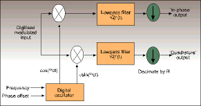
A downconverter consists of a numerically controlled digital oscillator, a mixer (shown as a pair of multipliers), and a low pass filter, as shown in Figure 1. The band-limited output from the filter allows us to reduce the sample rate by decimating. The design is fairly straightforward; although we must pay attention to the fidelity of the digital sinusoid-sine and cosine waveforms produced by the numerically controlled oscillator, we must also consider the quality of the filters if we are to have acceptable noise performance. (We must keep the design from adding so much noise to the incoming modulated signal that we cannot reliably detect it. How much noise is acceptable depends on the application.) Some digital radio applications have fairly high sample rates, which can make the design more challenging. With careful design, however, modern FPGAs can handle data as fast as any commercially available analog-to-digital converter can supply it. The advantage of using an FPGA is that it allows us to customise the DDC to exactly match our application. Furthermore, with an FPGA implementation, we can put the DDC and any post-processing in the same chip. Post-processing is usually some form of demodulator.
The oscillator
In terms of system performance, the critical component in digital downconversion is the numerically controlled oscillator (NCO). This component generates a sampled digital sinusoid, which when mixed with the incoming signal, shifts the signal's spectrum. In other words, if we multiply (mix) a signal with a sine wave, we get a frequency translation or 'shift' of the spectral image. The amount of translation is equal to the frequency of the 'carrier' sine wave.
Insufficient precision or accuracy in the sinusoid leads to degraded signal-to-noise ratios and to spurious spectral artifacts, either of which can swamp the incoming signal. Attention to the quantisation that leads to these noise terms is essential for the proper design of an NCO. In our implementation model, our NCO consists of a phase accumulator frequency synthesizer and a phase angle-to-wave shape conversion. The phase angle-to-wave shape conversion circuit may be any one of several possible designs.
The frequency synthesizer is simply an accumulator used to integrate a phase increment value. If we interpret the MSB (most significant bit) of the accumulator as having a weight of p then the accumulator represents the fractional portion of the accumulated phase angle. (Phase accumulator frequency synthesis is discussed in detail in an article by Austin Lesea at www.xilinx.com/xcell/xl31/xl31_32.pdf).
Using a phase accumulator offers several advantages over other methods:
* The synthesized frequency need not have an integer relationship to the sample clock, because modulo arithmetic preserves the fractional part of the accumulated phase on an overflow. This lets us set the local oscillator to an arbitrary frequency without changing the sample rate.
* The phase increment value does not have to be a constant. By dynamically changing the increment value, we can easily modulate the phase or frequency of the generated signal.
* Because 2N represents a full phase revolution, this generator interfaces nicely with look-up tables for wave shape conversion. Nothing in the phase accumulator design will impair the noise performance of the NCO; reducing word width only restricts the frequencies that can be synthesized.
Noise is generated by an imperfect rendition of the sinusoid at the output of the NCO. That noise can be phase errors (angular distortions) or amplitude errors. The phase accumulator generates only a phase angle, so there is no amplitude error. Errors caused by quantisation of the phase increment can cause a frequency error, but not a changing phase error.
Waveform synthesis
The phase accumulator produces a 'wrapped' phase angle that must be converted to a sampled complex sinusoid. The accuracy of the conversion directly affects the noise performance of the DDC. The noise introduced by the NCO is caused by amplitude and phase errors, which manifest themselves as reduced signal-to-noise ratio (SNR) and degraded spurious-free dynamic range (SFDR) respectively. Each additional bit of phase improves the SFDR by about 6 dB and extra amplitude resolution adds to the SNR by about 6 dB.
The most obvious conversion circuit is a simple look-up table of sine values by phase angle, which is addressed directly by the phase accumulator. The phase resolution determines the depth of the table, while the amplitude precision determines the width. To keep the size of the table reasonable without sacrificing frequency resolution, we must truncate the phase accumulator output, using only the MSBs at the cost of degrading the SFDR. The size of a table grows exponentially with phase resolution, so for even moderate SFDR requirements, the table becomes larger than what we would like to use in an FPGA.
Simple amplitude and phase symmetry allows us to reduce the table size by a factor of four by re-using the first quadrant data for the other quadrants. The same table is used for both the sine and cosine values, so if clock cycles, per sample permit, the same ROM can be read twice per sample. In the Xilinx Virtex devices, you can use the dual-port feature of the block RAM to simultaneously obtain both the sine and cosine values from a shared ROM. Large ROMs in FPGAs are expensive in terms of resources used so, for phase resolutions of more than 8 to 10 bits, other methods should be used.
The large ROMs can be avoided by algorithmically generating the sine and cosine on the fly. While that sounds difficult, there is a simple shift-add algorithm based on vector rotation called CORDIC (COordinate Rotation DIgital Computer) that makes this task fairly easy in hardware. (See www.andraka.com/cordic.htm) The algorithm simultaneously generates a sine and cosine value by rotating a unit vector from the 'I' axis to the desired phase angle using a series of successively smaller elemental rotations. The angles of those elemental rotations are specifically selected for a shift-and-add implementation. The 'I' (real or in-phase) and 'Q' (imaginary or quadrature) components of the rotated vector are proportional to the cosine and sine of the phase angle respectively.
The mixer
The function of the mixer is to multiply the incoming signal by the locally generated sinusoid to shift the spectrum of the signal. A straightforward implementation uses two multipliers, one each for the sine and the cosine. The multipliers produced by the CORE Generator tool can easily be used for this application.
If we use CORDIC for the wave shape conversion, however, we can obtain the mixer function for free. The combination of the NCO and the mixer multiplies the incoming signal by
Because the NCO and mixer generate a complex phasor, the net effect is to rotate the incoming signal by a constantly changing phase angle. Rather than rotating a unit vector to get I and Q scale values, we can use the CORDIC to directly rotate the input signal. This eliminates the two multipliers and avoids the potential for additional quantization noise.
A more subtle advantage to using CORDIC is that it actually rotates the vector rather than multiplying the components separately. This means it does not add noise to the signal other than the spectral spurs caused by the phase quantisation. The CORDIC hardware occupies about the same area as a pair of multipliers with the same input width in the Virtex architecture. Thus, in effect, we have a net area savings about equal to what we would have used for the sine and cosine wave shape conversion. The CORDIC rotator also accepts a complex input, so no additional hardware is needed for applications requiring a complex signal input.
The filter and decimator
The mixed signal has to be filtered to isolate the portion of the spectrum containing the signal of interest. The filter typically has to be a narrow-band filter with a fairly high rejection of unwanted spectrum. This translates to an expensive filter if it is done at the input sample rate. Instead, we can use a multi-rate approach in which the signal is first decimated to a much lower sample rate using a less computationally intensive filter. Then the signal is cleaned up with a second more complex filter working at the decimated sample rate.
High ratio decimator
A high-ratio decimation can be performed very efficiently using a cascaded integrator-comb (CIC) filter. The CIC filer is a recursive implementation of the 'boxcar' or moving average filter. The spectral response of such a filter is the sinc (sinx/x) function. In a CIC filter, the number of effective taps is an integer multiple of the decimation ratio, so the filter nulls alias onto the passband when the spectrum is folded by decimation. If the passband is sufficiently narrow, the rejection of the aliased image is quite good; much better than might be expected otherwise. We can also cascade several sections to lower the amplitude of the side lobes. The passband of this filter does exhibit a pronounced roll-off that usually must be corrected by the clean-up filter. Keeping the passband of the final filter narrow not only improves the alias rejection, but also makes the roll-off compensation easier.
The advantages of using a CIC filter in this implementation are:
* It is a computationally easy filter to realise.
* The same filter structure works for a very wide range of decimation ratios by simply changing the timing of the clock enables on the comb section.
* The filter response referred to the output sample rate is nearly independent of the decimation ratio, so one clean-up filter can be used for all decimation ratios.
The gain of the CIC filter is a function of the decimation ratio. Therefore, a barrel shifter is required after the CIC filter in applications where the decimation ratio has to be changeable without changing the circuit. This is an issue in an ASSP DDC, as it is a one-size-fits-all solution. Most of the time in FPGAs, we can hardwire the shift, or at worst, use a limited barrel shift, because we can customise the DDC for our application.
'Clean up' filter
The output of the CIC filter has a sinc shape, which is not suitable for most applications. A 'clean-up' filter can be applied at the CIC output to correct for the passband droop, as well as to achieve the desired cut-off frequency and filter shape. This filter typically decimates by a factor of two or four to minimise the output sample rate after the passband has been limited and shaped. An application-specific filter response, such as a raised cosine Nquist filter, can either be combined into the correction filter or be applied at a subsequent filter stage. The clean-up filter is compactly implemented using serial distributed arithmetic (see www.andraka.com/distribu.htm for a tutorial on distributed arithmetic).
Identical filters must be applied to both the I and Q channels. Even using the slowest speed grade Virtex FPGAs, the DDC design described here can be clocked at more than 130 MHz if the design is carefully executed and floor planned. This high potential clock rate permits us to time multiplex the I and Q data through the same filters by interleaving the I and Q samples on a clock-to-clock basis. Thus for very little additional overhead, we can handle both the I and Q data in the same filter. We can also use the same technique to handle several independently tuned channels with a single instance of the DDC design.
An advantage of using an FPGA for the DDC is that we can customise the filter chain to exactly meet our requirements. With an off-the-shelf chip, we would have to either fit our requirements to the chips' features or add additional post-processing to modify the output to our needs.
Conclusion
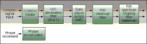
We have briefly discussed implementation of a high performance DDC in an FPGA. If we apply these techniques to a 16 bit DDC with a 64 MS/sec input and a 100 dB SFDR requirement, we come up with a design that occupies about 550 Virtex CLBs (configurable logic blocks). The occupied area is heavily influenced by specific requirements of the application. The cited design, shown in Figure 2, consists of an NCO and mixer implemented as a CORDIC rotator and a programmable decimating filter. The filter is a 4th order CIC filter followed by a 63-tap symmetric finite impulse response (FIR) filter. Backing off on any of the requirements can substantially reduce the area occupied by the DDC. Because we are using an FPGA, we have the luxury of picking the features and performance to match our application. If we were to use an ASSP component, we would have to mould our requirements and design around the capabilities of the selected device.
For further information about Xilinx contact Avnet Kopp, (011) 444 2333, sales@avnet,co.za, or www.avnet.co.za


© Technews Publishing (Pty) Ltd | All Rights Reserved
 printer friendly version