


The first half of this article appeared in the 12 June edition of Dataweek.
Typical parameters of importance for references
Initial accuracy speaks for itself: it is the value set by any trimming. One can take a part off the shelf, connect it in a test circuit in automatic test equipment (ATE) and measure the output voltage. The measured value should be within the initial accuracy tolerance specified in the data sheet.
This specification is usually for room temperature only, with a defined input voltage and load current. It provides a starting point for most of the other specifications. Initial accuracy tolerance can be affected by package stress, so proper control of the solder temperature profile is essential and twisting of the PCB must be kept to a minimum.
Because package stress may start to change the unpowered part on the shelf, the initial accuracy tolerance may be subject to slight drifts; see the sections ‘Temperature hysteresis’ and ‘Long-term drift (stability)’ below. This is one reason why many industries, notable the military, require new products with date-coded parts to be less than a certain age.
Temperature coefficient (tempco) is the deviation of reference output voltage due to a change in the ambient or package temperature. Depending on the device structure and the way its output voltage is trimmed during the initial calibration, this output-voltage deviation can be positive (increasing with increasing temperature) or negative (decreasing with increasing temperature). It is almost never linear with temperature, which sometimes leads to confusion.
For example, a temperature change from 25°C to 30°C is unlikely to lead to the same output voltage change as a temperature change from 65°C to 70°C, although the temperature increase is the same. By analogy, consider a simple resistive voltage-divider (Figure 4A). Voltage at the common point (VOUT) is a fraction of the applied voltage (VIN) equal to the ratio of the values of the two resistors. Both resistors change with temperature by the same percentage, maintaining a constant ratio, so VOUT also remains constant.
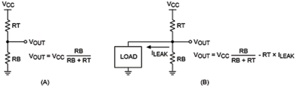
Note that current flowing through the resistors varies with the temperature, and any leakage current from the common point of the divider (positive or negative) changes VOUT (Figure 4B). At room temperature, this change is usually compensated for by trimming one of the resistors (changing its value). However, if this variation of leakage current with temperature differs from the variation in divider current due to changes in the resistor values with temperature, then the result is a change in VOUT with temperature.
The VOUT change is called the temperature coefficient, or tempco. Although this analogy simplifies the more complex mechanism inside a reference circuit, it conveys the idea of a device tempco.
Temperature hysteresis is the change in output voltage with a cycle of temperature variation. To measure this, take a reference operating in a typical application, rated (as an example) for the extended operating temperature range of -40°C to +85°C. Record the output voltage at room temperature (+25°C). Cool the reference to -40°C and then heat it to +85°C before returning it to
25°C. Measure and record the output voltage again.
The difference in these measurements, if any, is the temperature hysteresis. Note that it is also valid to heat it to 85°C, cool it to -40°C, and then heat it to 25°C. The deviation can be positive or negative. After many temperature cycles, one might deduce that the reference output voltage can be quite different.
Because temperature hysteresis is both positive and negative, however, the deviations resulting from a series of temperature cycles tend to cancel out each other, producing a final average output voltage very close to the nominal value. This parameter is associated with stress on the die.
Heat cycling tends to equalise the stress; typically after five cycles, the stress has decayed to a minimum. However, stress can be reintroduced by soldering or twisting the package.
Line regulation is a measure of the change in output voltage due to a change in input voltage. This is important if the input voltage changes while the reference is operating, such as in a battery application. Typical units are ppm/V and %/V.
Line regulation is a DC parameter and is typically specified at DC. Line regulation measures the change in output voltage for two (or more) different DC input voltages; it has little meaning if the input voltage varies rapidly, as for a voltage transient.
In general, line regulation deteriorates inversely with the rate at which the line voltage changes. For applications likely to have line transients, reference input capacitors are recommended to minimise the resulting variations.
Load regulation is a measure of the change in output voltage due to a change in the reference load current. This parameter is important if the reference load current changes while the reference is operating, e.g., when a reference is driving a resistive ladder-type DAC with no reference buffer. The ladder impedance changes significantly with the DAC code.
Again, load regulation is a DC parameter and is typically specified at DC. It measures the change in output voltage for two (or more) different DC load currents, and it has little meaning if the load current varies rapidly. In general, load regulation deteriorates inversely with the rate at which the load current changes.
Output capacitors are recommended to stabilise the output voltage in applications subject to load-current transients. Typical units of measure are ppm/mA, %/mA and percent change from no load to full load.
Long-term drift (stability) is important if the reference must remain accurate for days, weeks or years of continuous operation. It simply measures the variation in output voltage over a long period of time at some specified condition of steady-state operation.
Long-term drift is a measure of the maximum and minimum output-voltage deviations over an extended time period, rather than a measure of deviation between time A and time B. All other conditions (e.g., temperature, input voltage, load current) must be held constant if this measurement is to accurately reflect drift in the reference. Typical units are ppm per 1000 hours.
Supply current is self-descriptive, but consider these variations:
For a series reference, the term ‘no-load current’ is usually specified in the datasheet and often used interchangeably with the term ‘quiescent current’ (IQ). Because it designates the actual current drawn by an unloaded reference, no-load current does not specify the current drawn by that reference when loaded.
Typical shunt references do not specify no-load current in the datasheet. Instead, they often list a minimum operating current (IMO). This parameter specifies the minimum current that a reference must draw to maintain regulation.
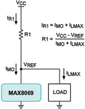
Note that a shunt reference must draw at least the minimum operating current under full-load conditions. Its series resistor (R1) must, therefore, accommodate the maximum load current plus the minimum operating current (Figure 5). In some applications, the minimum operating current (called ‘regulation current’ in some datasheets) is disregarded because it is so much smaller than the load current.
Ground current is often specified for a series reference. It measures the operating current at a given load. A series reference is in series with the load, so a measure of current flowing into the reference input yields the sum of load current and operating current. Ground current is often measured to determine the operating current for a series reference with load.
Dropout voltage (VDO) is very important in low-voltage and battery-operated equipment and applies only to the series reference (in series references, this is the same as IMO discussed above). The minimum difference between input and output voltage is what allows the reference to maintain its specified accuracy (VOUT + VDO = minimum input voltage).
Battery voltage declines as the battery discharges. To maximise useful life in the battery, the reference must maintain an accurate output voltage while powered by the lowest possible battery voltage. Thus, a lower dropout voltage allows continued operation at a lower battery voltage.
Pay close attention to the current at which the dropout voltage is specified. A dropout voltage at zero current gives an artificially low value. This is comparable to drawing a small current when a rail-to-rail output approaches the rail.
Load capacitance is the ability of a reference to drive capacitive loads, and it can be very important. Because typical references incorporate feedback control, their stability can be compromised by the zero introduced by a capacitive load. This can produce a large phase shift in the control loop that creates positive feedback at a particular frequency.
Read the datasheet carefully for information on the range of load capacitance allowed. Some manufacturers refer to this limitation only in the text of the datasheet and not in the parameter tables.
Noise is apparent at a reference output, but it is, nonetheless, often overlooked. A reference’s noise, which is a random signal generated by active and passive devices inside the IC, affects its accuracy. For example, a 1 mVP-P output noise voltage limits initial DC accuracy to no better than 1 mV. For a 1,2 V reference, this noise level alone limits initial accuracy to approximately 0,1%.
Reference datasheets typically show noise in two frequency bands: low-frequency noise, ranging from 0,1 Hz to 10 Hz and specified in μVP-P; and wideband noise, ranging from 10 Hz to 1 kHz and specified in μVRMS.
Designating noise in two bands allows circuit designers to distinguish between wideband noise, which they can filter with practical capacitor values, and low-frequency noise, which they cannot. Also, if a capacitor large enough to filter the low-frequency noise were used, the reference could be unstable with such a large capacitor placed at its output.
AC line regulation is not usually designated in a specification table, but it directly influences the performance of the voltage reference. In most applications, the supply voltage to the reference has voltage spikes present. These spikes tend to be spread over a wide frequency range. The accuracy of the voltage reference is inversely proportional to the frequency of the input voltage variation.
Because the AC line regulation is typically not specified, the reference datasheet should at least contain a graph showing the typical AC line regulation versus frequency. This graph would indicate the sensitivity of the reference to input system noise, and could be used to determine the input filtering required. As the noise frequency increases, the input filtering must further reduce the input system noise so the reference can achieve its rated accuracy.
Power-supply rejection ratio (PSRR) is sometimes specified in a datasheet, usually in dB. It is a measurement of how much noise is rejected by the part at the output from the input supply (PSRR = ΔVCC/ΔVOUT).
AC load regulation/output impedance is another important parameter often omitted in the specification table of a voltage reference. This parameter is important if the load current drawn from the reference is constantly changing. The accuracy of the reference is usually inversely proportional to the load variation frequency.
A graph showing the AC load regulation or AC output impedance versus frequency should be contained in the reference data sheet. This graph should show what output filtering is required with the known output load variations to achieve the rated accuracy of the voltage reference.
Line transient response is typically shown as an oscilloscope screenshot displaying a step change in the input voltage and the resulting change and correction in the output voltage. This screenshot displays the recovery time of the reference returning to a specified accuracy after such an event. It is important to note the input and output capacitor values used. These capacitors have a tremendous effect on the performance of the reference.
Load transient response/output settling time is typically shown as an oscilloscope screenshot displaying a step change in the output current and the resulting change and correction in the output voltage. This screenshot displays the recovery time of the reference returning to a specified accuracy after such an event. It is important to note the input and output capacitor values used. These capacitors have a tremendous effect on the performance of the reference.
Turn-on/turn-off settling time. The turn-on settling time is a measure of how quickly the output voltage of the reference stabilises after an initial power-up. The output only needs to be stable and may not necessarily have reached the specified accuracy of the reference. Typically, this parameter is specified with an output voltage error greater than the specified accuracy; it should always be given in the conditions of the parameter.
This parameter is highly dependent on the input and output capacitor values used and the load applied to the reference. It is not uncommon for references to encounter their current limits at power-up, when they have to charge up all their load capacitance.
Turn-off time is a simple measure of how long it takes for the output voltage of the reference to virtually reach zero volts. This parameter is also highly dependent on the input and output capacitor values used and the load applied to the reference.
Output short-circuit current is a protection feature that can be either a short to GND or a short to input. It is a measurement of the output current when the output pin is shorted to either GND or IN. Typically, this is a fault condition which the part will enter under maximum thermal stress. In the Absolute Maximum Ratings section of a data sheet, a time duration is shown to specify how long the part can operate in this condition.
Conclusion
Voltage references are often chosen in haste. Before making a decision, the designer will look at the price, the initial accuracy highlighted on the datasheet, and frequently nothing else. Designers should make sure to compare apples with apples when comparing references.
When evaluating a specification listed on several datasheets, be sure that all are expressed in the same units. Determine what parameters are important for the application, and look beyond the initial accuracy specifications.
| Tel: | +27 11 608 0070 |
| Email: | [email protected] |
| www: | www.cstelectronics.co.za |
| Articles: | More information and articles about CST Electronics |


© Technews Publishing (Pty) Ltd | All Rights Reserved
 printer friendly version