


Everyone has encountered electrostatic discharge (ESD) after walking across a room with a woollen carpet and touching a metal doorknob. The experiment with cat fur and a resin rod is also a good demonstration of this. ESD is the dissipation of static electric charge, which results in a charge flow from higher to lower potential. Unfortunately, such charge may be transferred from a human hand to the connector pin of an I/O port of an electronic circuit where it can reach an IC and cause permanent physical damage.
This article discusses the ramifications of this problem, defines testing methods and standards for ESD, and provides insight on solutions to the problem using a rather unique product in an application where ESD might not be thought of as a major source of problems.
Discussion
The increase in the availability of consumer electronic products over the years has resulted in a drive for reduced PCB real estate, increased component integration, increased signal speed, and reduced component size. EMC standards have become increasingly important in recent years. These require that electronic products exhibit immunity to ESD exposure and reduced EMI/RFI susceptibility/radiation.
ESD exposure can cause permanent damage in the form of oxide breakdown, shorts, opens, or latch-up. Temporary problems may be latch-up or ground bounce. Latent damage can also occur in the form of degradation due to an ESD event.
A thinning of gate oxides for MOSFET products has resulted from the scaling down of devices in order to increase the performance (speed) and packing density. The thinner gate oxide means a lower dielectric breakdown voltage. A good rule of thumb for dielectric breakdown voltage is between 60 to 80 V per 1000 ≈ of gate oxide. The thickness of the gate oxide on current generation 0,35 µ CMOS is about 100 ≈. This means the oxide can rupture at a voltage of around 6 to 8 V. As the next generation of 0,28 µ CMOS has around 70 ≈ of gate oxide thickness this gate rupture voltage is expected to decrease.
Most CMOS ICs have some form of built-in ESD protection to protect the devices against ESD occurring from handling during the equipment manufacturing process. This built-in ESD protection is typically designed for 2 kV of human body model (HBM) ESD protection. Since this level of protection is meant to work in conjunction with the fact that the manufacturing environment is already somewhat equipped to handle ESD exposure the ICs are still vulnerable in other real-world situations. Since such components may be exposed to ESD after being built into a system or an end product, it is necessary to provide additional external ESD protection to them.
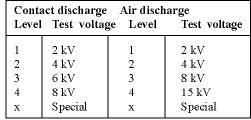
Field failures caused by ESD also pose problems. It can obviously be very costly to repair such failures by replacing defective components or equipment. Incorporating ESD tolerance into electronic equipment helps to reduce or eliminate such undesirable situations. ESD protection requirements at the system level have increased. It is now common to require IEC-61000-4-2 ESD compliance at level 4 (8 kV contact discharge) rather than the previously required 2 kV HBM compliance.
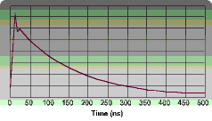
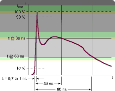
Because of a difference in test set-up requirements, the IEC model delivers approximately 50% more energy and has approximately five times the peak current in the ESD pulse than the HBM at a given voltage.
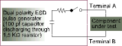
The difference in ESD transmitted using the two tests is due to the basic difference in test set-ups. With the HBM, a 100 pF capacitor is charged up to a test voltage and then discharged through a 1,5 kOhm resistor (Figure 3). The test is conducted using two sets of three pulses, one going high and the other going low. The IEC 61000-4-2 method charges a 100 pF capacitor but then discharges the signal through a 330 Ohm resistor, resulting in a higher level of energy being delivered to the device under test (DUT) (Figure 4).

Protection techniques vary. Clamp diodes in an IC are often insufficient. Shielding provides a low level of effectiveness, while bypass capacitors or series resistor/inductors can degrade signals, and require many components. Spark gaps are a low cost solution but provide low stability while requiring a large board area. Discrete zener diodes provide high capacitance and also require many components to implement. Discrete PN diodes offer a lower capacitance but again require many components.
Integrated diode networks are often the optimum solution since they provide superior downstream ESD protection with a high-speed response; the ESD current is steered to ground or VCC. Any signal degradation is minimised due to low capacitance. These require a minimum of board space with low assembly and manufacturing costs. The design time to implement such solutions is minimal and they provide long-term reliability.
To illustrate a specific application where ESD protection is required, and where an integrated solution is used, a product that interfaces a video controller to the video port will be discussed. The interface requires ESD protection for all signals connected to the VGA port pin, precision matched R/G/B video DAC termination resistors for colour fidelity, H-Sync and V-Sync signal boosting/buffering essential for picture quality at high resolution and display data channel (DDC) signal level shifting.
The particular solution discussed here is the VGA port companion circuit (PACVGA200) made by California Micro Devices. This device provides seven channels of ESD protection for all VGA port connector pins and it meets IEC-61000-4-2 level 4 ESD requirements (8 kV) contact discharge. The PACVGA 200 offers low loading capacitance from the ESD protection diodes on video lines (4 pF typical) which ensures maintenance of the integrity of the video signal.
This solution features TTL to CMOS level-translating buffers with power-down mode for HSYNC and VSYNC lines and the required 75 Ohm termination resistors. The termination resistors are typically matched to 1%. Integrated bi-directional level shifting N-channel FETs are provided for DDC_CLK and DDC_DATA channels. The ESD protection for the VGA port signal lines is implemented with current steering diodes designed to safely handle the high surge currents encountered with IEC-1000-4-2 level 4, 8 kV contact discharge. When a channel is subjected to an electrostatic discharge, the ESD current pulse is diverted via the protection diodes into the positive supply rail or ground where it may be safely dissipated. All of this is included in a compact 24-pin QSOP package.
An internal diode is also provided so that Vcc3 can be derived from Vcc4, if desired, by connecting Vcc3 to V_BIAS. In applications where Vcc4 may be powered down, diode D1 blocks any DC current paths from the DDC_OUT pins back to the powered down Vcc4 rail via the top ESD protection diodes.
Applying the PACVGA200
A resistor may be necessary between the Vcc3 pin and ground if protection against a stream of ESD pulses is required while the PACVGA200 is in the power-down state (Figure 5). The value of this resistor should be chosen such that the extra charge deposited into the Vcce bypass capacitor by each ESD pulse would be discharged before the next ESD pulse occurs. The maximum ESD repetition rate specified by the IEC-61000-4-2 standard is one pulse per second. When the PACVGA200 is in the power-up state, an internal discharge resistor is connected to ground via a FET switch for this purpose.
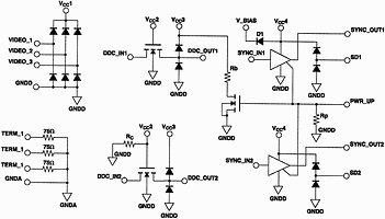
For the same reason, Vcc1 and Vcc4 may also require bypass capacitor discharging resistors to ground if there are no other components in the system to provide a discharge path to ground. GNDA, the reference voltage for the 75 Ohm resistors is not connected internally to GNDD and should ideally be connected to the ground of the video DAC IC.
This product can be used on add-on PC display adapter cards, notebook computers with VGA port for external monitors and PC motherboards with embedded video controllers.
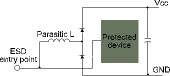
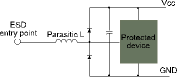
While the previously described device serves a very specific ESD protection function, CAMD makes other ESD protection devices which have more generic protection features. The number of channels ranges from 2 to 18. One very important thing to keep in mind is the placement of the ESD protection device. In order to reduce the possibility of series inductance overriding the ability of the protection devices to behave accurately, it is very important to place the ESD protection device as close to the exposure port as possible, as shown in Figure 6. The illustration is an example of poor layout. Such a layout would indicate poor ESD protection. The layout in Figure 7 is preferred. The energy from an incident ESD pulse would be quickly dissipated to Vcc or ground through the capacitor connected across the protected device. It is necessary to utilise the PACVGA200 with this layout, as the product will not operate properly without placing an external capacitor in the circuit in this manner. Place a ceramic bypass capacitor (90,1 to 0,2 µF) as shown.
Conclusion
ESD is a growing problem in the electronics world and is being addressed by an ever-increasing number of device vendors with increasing complexity and functionality. Care must be taken in placement of the ESD protection device on the PCB relative to the point of insertion of the ESD.
For further information contact MB Silicon Systems, (011) 728 4757, [email protected]
| Tel: | +27 11 728 4757 |
| Email: | [email protected] |
| www: | www.mbsiliconsystems.co.za |
| Articles: | More information and articles about MB Silicon Systems |


© Technews Publishing (Pty) Ltd | All Rights Reserved
 printer friendly version