Product development issues explored in new video
27 March 2019
Manufacturing / Production Technology, Hardware & Services
Printed circuit broker, Elmatica, recently released a new film about product development, explaining why cooperating with an experienced partner could be a smart move.
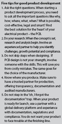
“We have several times seen the unfortunate result of inadequate planning and execution in the early phase of the product development process, explains the company’s CEO, Didrik Bech. “Early involvement of an experienced partner in the design phase can save you from costly mistakes. This new movie is meant to inspire all parties involved in product development, and bring attention to doing things correctly, from the beginning. At Elmatica we value transparency and sharing knowledge, we are not reluctant to share our know-how or ask the challenging questions.”
The animated movie (accessible at www.youtube.com/watch?v=kGFJvLBqmCE) follows a product, this time a robot, from when the idea is hatched in the designer’s head until the finished product is loaded safe and sound on an aeroplane towards the end customer. The whole process is supported by the printed circuit broker.
“The product development process is broken down as a six-step process from idea generation to launch. We want to focus on how close cooperation with an experienced partner, which knows PCBs by heart, can improve the process and ensure that cost and time saving elements are considered in all phases,” says Bech.
Changes in the supply chain
Elmatica has supported the development of thousands of products since its establishment in 1971. Even if the process is more or less the same in 2019 compared to 1971, some things have changed as several companies have outsourced parts of their supply chain and products have increased in complexity, with the result that many are often more reliant on external knowledge and specialists.
“We have organised our products to match different parts of your development process. This makes it easier for you to understand what we do, and for you to decide when and how you would like to include us. In this movie, we show how each of our products can fit with your product development process, supporting it from the beginning until the end, delivering technical assistance, auditing, experience, seminars and contacts,” says Bech.
For more information visit https://elmatica.com/contact/
Further reading:
World-first 016008 mm component placement
Manufacturing / Production Technology, Hardware & Services
Fuji has achieved the world’s first placement of 016008 mm (0,16 x 0,08 mm or 006 x 003 inches) size components on printed circuit boards with its SMT pick and place machine, NXTR.
Read more...
Lifecycle and obsolescence: Protecting electronics through process
Production Logix
Manufacturing / Production Technology, Hardware & Services
At Production Logix, we believe longevity is not accidental. It is engineered through early visibility, structured response, and disciplined execution, in partnership with our OEM customers.
Read more...
Maximising squeegee quality and durability
Testerion
Manufacturing / Production Technology, Hardware & Services
Transition Automation has announced two new product advancements designed to improve SMT printing performance and extend squeegee life: laser-enhanced Permalex bonding and integrated edge protectors.
Read more...
NeoDen ND2 PCB screen printer
ZETECH ONE
Manufacturing / Production Technology, Hardware & Services
The NeoDen ND2 PCB screen printing machine is a fully automatic stencil printer designed to deliver precise and consistent solder paste application in modern SMT production environments.
Read more...
Understanding the BGA rework process
Techmet
Manufacturing / Production Technology, Hardware & Services
BGA rework is a highly technical process that involves removing the faulty component, preparing the circuit board, and installing a new or repaired device, while maintaining the integrity of the printed circuit board.
Read more...
Flexible three-process reflow soldering system
Truth Electronic Manufacturing
Manufacturing / Production Technology, Hardware & Services
By combining multiple soldering technologies within a single system, the Vision TripleX system enables manufacturers to adapt easily to different assembly requirements, board designs, and production volumes.
Read more...
Inline vapour phase soldering for high-volume production
MyKay Tronics
Manufacturing / Production Technology, Hardware & Services
The VP2200-100 vacuum inline vapour phase soldering system from ASSCON is designed for fully automated, high-volume electronics manufacturing where process consistency and solder joint quality are critical.
Read more...
Global electronics solutions since 1964
IMP Electronics Solutions
Manufacturing / Production Technology, Hardware & Services
Over more than six decades, IMP Electronics Solutions has built a reputation for technical expertise, reliable supply chains, and strong partnerships with both customers and manufacturing partners.
Read more...
Driving excellence in electronics manufacturing
Jemstech
Editor's Choice Manufacturing / Production Technology, Hardware & Services
Jemstech’s reputation for disciplined execution and client-focused service has earned it strong loyalty from companies operating in demanding industries.
Read more...
When do you need Nitrogen in reflow?
Truth Electronic Manufacturing
Manufacturing / Production Technology, Hardware & Services
Nitrogen in reflow soldering is often seen as a performance enhancer, offering improved wetting, shinier joints, and fewer defects. But it is not always necessary.
Read more...


 printer friendly version