Differential signalling to clock faster, better control EMI, and accomplish long-haul serial transmission
10 April 2002
Telecoms, Datacoms, Wireless, IoT
Robert Hanson, American Seminars
As transmission speeds increase (10 gigabit SERDES, gigabit Ethernet, etc) there is greater need for high-speed serial transmission methods - usually Differential Signals (DS) for many companies. However, one must be aware that it has design restrictions that must be adhered to for successful design.
Here we look at the main requirements for DS, ie overcoming differential unbalance, controlling crosstalk, and providing the correct PCB layout.
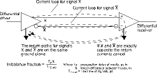
Figure 1. The ideal DS transmission
Differential unbalance
The ideal DS transmission is seen in Figure 1. If the two pathways are the same electrical length (EL), the return currents cancel. What would happen if they are not the same EL? The unbalance fraction is defined in Figure 1. When one edge arrives before the other, the return currents will not cancel until the second edge arrives. During this time, two detrimental effects will occur, a reflection on the line of the first arriving signal and crosstalk between the lines. Therefore, the layout personnel must be cognisant of these scenarios:
1. Propagation delay - (about 140 ps/in. outer layer, 180 ps/in. inner layer)
2. Vias - Each time a trace is disrupted by a via, the inductance of the total path is increased, thereby changing the EL.
3. Keep always - If one trace has to deviate around a pin, via, anti-pad, etc, the EL will be affected.
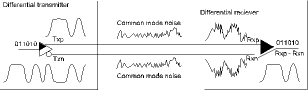
Figure 2. An example of noise (crosstalk) coupling into a differential pair
Crosstalk
Figure 2 defines an example of noise (crosstalk) coupling into a differential pair. Now, if the noise is only coupled to one and not the other, the receiver output data is useless.
Differential signals use two lines driven with complementary waveforms. A virtue of differential signals is that most noise sources couple roughly the same noise onto both lines. The differential receiver is designed to ignore signal components that are common to both lines (the common mode) while responding to the difference between the two lines (the differential mode), rejecting the coupled noise. A related benefit of differential signals is that the electromagnetic interference (EMI) generated by each line in the differential pair is largely cancelled by the other line.
PCB layout
There are three methods for laying out differential pairs: asymmetric; dual (broadside); side-by-side (edge).
Dual is very hard to accomplish due to accuracy of lamination process (x, y, and O errors among layers). The tradeoffs between dual and edge are:
* Side-by-side routing distances dual-distance and via length's electrical length.
* Three layer versus two layer lamination accuracy.
* Etching on 2 Cu planes versus 1 Cu plane.
Most companies will design using on-the-edge layout with the two sheets of Cu being ground planes. A major key to successful DS is careful planning of layout for EL and signals that are protected by the ground layers.
Robert Hanson will be delivering high-speed digital design seminars in South Africa during June. Contact [email protected], for further details.
Further reading:
SMT-mountable card connectors
Telecoms, Datacoms, Wireless, IoT
Würth Elektronik introduces four new SMT-mountable Nano SIM and microSD card connectors and expands its range with solutions for the smallest packages.
Read more...
Module for smart city and smart utility devices
iCorp Technologies
Telecoms, Datacoms, Wireless, IoT
Quectel Wireless Solutions has launched the Quectel KCM0A5S, a high-performance Wi-SUN module designed for smart applications such as street lighting, precision agriculture, industrial IoT, smart meters and smart cities.
Read more...
Ultra-low-power wireless module
Altron Arrow
Telecoms, Datacoms, Wireless, IoT
The STM32WBA5MMG from STMicroelectronics is an ultra-low-power, small form factor, certified 2,4 GHz wireless module that supports Bluetooth LE, Zigbee 3.0, OpenThread, and IEEE 802.15.4 proprietary protocols.
Read more...
Quectel partners with GEODNET
Quectel Wireless Solutions
Telecoms, Datacoms, Wireless, IoT
Quectel Wireless Solutions has partnered with GEODNET to deliver Quectel’s Real-Time Kinematic (RTK) correction services, enabling high-precision positioning for IoT applications.
Read more...
Bringing Bluetooth Channel Sounding to automotive and beyond with KW47
Altron Arrow
Telecoms, Datacoms, Wireless, IoT
NXP’s new Channel Sounding-certified KW47 and MCX W72 wireless MCUs are set to help automakers with distance measurement, bringing an additional ranging solution for car access and autonomous systems, and will be utilised across a broader spectrum of applications.
Read more...
Dual-band GNSS antenna
RF Design
Telecoms, Datacoms, Wireless, IoT
The Taoglas Accura GVLB258.A, is a passive, dual-band GNSS L1/L5, high-performance antenna for high precision GNSS accuracy and fast positioning.
Read more...
What is Wi-Fi HaLow and why choose it for IoT?
iCorp Technologies
Editor's Choice Telecoms, Datacoms, Wireless, IoT
Wi-Fi HaLow introduces a low power connectivity option that, in contrast to other Wi-Fi options, offers greater range of approximately 1 km, which opens up a raft of IoT use cases.
Read more...
Wi-Fi 6 and Bluetooth LE coprocessor module
Altron Arrow
Telecoms, Datacoms, Wireless, IoT
The ST67W611M1 from STMicroelectronics boasts an all-in-one design which, together with its capabilities, contribute to making it an attractive choice for IoT edge devices requiring a single-chip solution.
Read more...
Futureproofing IoT connectivity
SIMcontrol
Telecoms, Datacoms, Wireless, IoT
A managed private APN assigns every device to an isolated carrier slice, producing a single ingress to the enterprise network, with traffic bypassing shared internet paths and reducing exposure.
Read more...
Extra slim 2,4 GHz radio module
Telecoms, Datacoms, Wireless, IoT
The Thyone I radio module from Würth Elektronik now has a little sibling: Thyone-e, which takes up 30% less space and represents a cost-effective alternative for applications in which the long-range mode is not required.
Read more...


 printer friendly version