


When measuring shielding effectiveness, designers must take all issues into account.
The last five years or so has seen an increase in the use of the board-level shield, thanks to cost and size constraints posed by today's electronic products. In the past, 'shielding effectiveness' usually meant the ability of a shield to block uniform far-field electromagnetic radiation or energy.
Now, however, it is no longer sufficient to just throw out a number - it must be accompanied with sufficient conditions and understanding of the specific application.
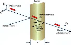
The most common definition of shielding effectiveness (SE) is
SE = 20 log (Ea /EI ) = 20 log (Ha /HI ),
where EI, HI are the electric field component and the magnetic field component, respectively, of the incident electromagnetic field, and Ea, Ha are the electric field component and the magnetic field component, respectively, of the attenuated electromagnetic field on the opposing side of the shield barrier.
Unfortunately, this equality is only true when the incident and attenuated fields are both uniform plane waves measured in the far field, and the barrier is of infinite proportions in all directions. Being in the far field is a condition where the electric field component and the magnetic field component are related by the constant 377 Ohm (120 pi Ohm), which is the impedance of air or free space.
However, this definition cannot be used for a general case other than for the far-field condition. Shielding effectiveness must be specified not only for normal far-field emission/immunity conditions, but also for near-field emission condition; near-field immunity condition; electric field lines or magnetic field lines; and finally frequency.
Near-field effects
Many complications occur when the shield is in the near field of the source. The electric and magnetic field components of the sources inside the shield will be different and must be considered separately. Performance will be impacted by the frequency and position of the source, the field configuration, and the parasitic or distributed inductances and capacitances.
With this approach, the aspect of the field (electric or magnetic) of interest in the shielding application must be known. However, this implies that we are still considering the field to be a radiated uniform field even in close proximity to the source. Also, being in the near field means an additional radial vector component of the field appears.
The stated simplified approach does not take this manifestation into account. In other words, the approach now becomes a 'coupling' problem because we are in the 'reactive' field area, which by itself indicates that it should no longer be considered a simple radiated problem. Even accounting for shield apertures, calculating or estimating shielding effectiveness of a shielded enclosure or box could still fall short of approximation.
The coupling of the source to the shield, the effect of mutual coupling between elements, the effect of the shield termination, and the grounding technique all need to be taken into account. We must consider induced currents and their return paths, currents diffusing through the shield, shield discontinuities (that is, bends and corners), and the resultant generated external voltages.
The effectiveness of the board-level shield is highly dependent on the proper design of the PCB mounting area. Normally, the sixth side of this shield will be a ground plane on the board. The number and the spacing of vias and/or traces running from this shielded area to other board components can affect the effectiveness of the shield.
So more is involved than just placing a can over the device or circuit to get the most benefit from using board-level shields. The designer must not forget about the various noise-escape paths through the interlayer traces, vias, pads and holes.
Avoiding coupling
Vias, pads and holes are very inductive at high frequencies, and the voltage drop across them could couple to the shield and nearby traces. Accordingly, it is important that the shield extend beyond the vias, pads and holes to avoid coupling from these fringing fields, covering not only the device, but these escape routes as well. The same warning also applies to ground moats and segmented power planes.
However, with higher frequencies and shorter wavelengths, the size and number of holes are becoming an issue. The dimension of these holes decreases the shielding effectiveness as wavelengths approach these same dimensions, as a sample calculation shows.
Let's assume a frequency of 100 GHz and a corresponding wavelength of 3,05 mm. Typically, apertures and holes should be no larger than 1/20th to 1/50th of the wavelength, that is, 0,153 to 0,061 mm (0,003 to 0,006 in). In other words, we cannot have any apertures, holes, or seams any larger than 3 to 6 mils in diameter or length.
Therefore, one can see how difficult it becomes at higher frequencies to completely seal up a board-level shield. Other methods need to be used, such as absorber materials.
Other considerations
Another issue with higher frequencies is resonance effect. Its coupling is a consequence of self-resonance of various structures such as reactively terminated transmission lines, slots in the PC board, slots between the PC board and metallic enclosure, all of which can behave as cavity resonators.
A 2 x 12,7 mm enclosure resonates at a first-order mode of around 12 GHz. Even weak coupling at these extremely high frequencies may induce strong oscillations that can couple to other points in the enclosure. To reduce this phenomenon, the Q factor of the cavity must be lowered by introducing losses (Q dampening).
Absorber materials are a viable option for handling frequencies greater than 1 GHz. They reduce radiation by literally absorbing the energy and converting it to heat. Since they convert the electromagnetic energy, these materials do not have to be grounded. As long as they intercept or are in the field path, they will reduce the electromagnetic energy of the field.
So in the future, shielding will become more and more of a multilevel concept. Board-level shields will handle the lower frequencies as usual, and an internal layer of absorber coating will handle the much-higher-frequency components.
At frequencies greater than 10 GHz, surface conductivity becomes increasingly critical because of a phenomenon known as skin effect, in which currents tend to crowd into the uppermost layers of a conductor. As more and more current crowds into less and less thickness, current density increases, which in turn produces an increased voltage drop and the potential for more radiation or leakage.
The surface conductivity of the finishing layer or gasket material becomes critical. Manufacturers are already experiencing this with protective finishes used on their enclosures because some protective finishes such as zinc chromate are composed of conductive particles in a binder material.
Another problem with various finishes is that a minimum pressure is required to obtain low surface contact resistance. Data is currently being gathered to understand this phenomenon better.
For further information contact Laird Technologies' local representative, Connecta, 011 463 2240.


© Technews Publishing (Pty) Ltd | All Rights Reserved
 printer friendly version