


Ref: z2511084m
Establishing a new benchmark for speed and RF phase-noise performance, the ADF4106 phase-locked-loop synthesizer is fully specified to operate at frequencies up to 6,0 GHz. This allows designs for the 5,4 GHz to 5,8 GHz upper ISM band to be greatly simplified. This device displaces the pin-and software-compatible 4 GHz ADF4113 as the fastest available integer-N synthesizer - and can achieve 3 dB lower phase noise to boot!
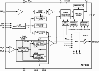
The ADF4106 frequency synthesizer requires only a 3,3 V supply, yet its VP pin is specified at up to 5,5 V for compatibility with tuning voltage levels often required by modular VCOs used in basestations. The device (Figure 1) can be used to implement local oscillators (LOs) in the up- and down-conversion sections of wireless receivers and transmitters. It consists of a low noise digital phase frequency detector (PFD), a precision charge pump, a programmable reference divider, programmable A and B counters, and a dual-modulus prescaler (P/P + 1). The A (6 bit) and B (13 bit) counters, in conjunction with the dual-modulus prescaler (P/P + 1), implement an N-divider (N = BP + A). In addition, the 14-bit reference (R) counter allows selectable REFIN frequencies at the PFD input. A complete phase-locked loop (PLL) can be implemented if the synthesizer is used with an external loop filter and voltage-controlled oscillator (VCO). Its very high bandwidth means that frequency doublers can be eliminated in many high-frequency systems, simplifying system architecture and lowering cost.
Wide bandwidth allows it to function as a 6 GHz local oscillator
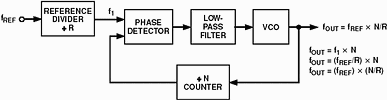
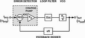
The standard PLL system architecture used by the ADF4106 and its predecessor, the ADF4113, is shown in Figure 2.
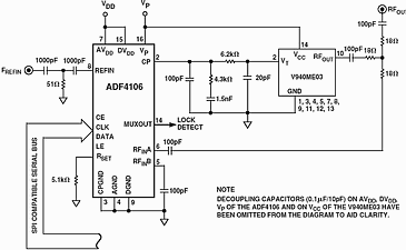
Since the maximum operating frequency of the ADF4113 is about 4 GHz, higher frequencies require the use of a frequency doubler - which usually calls for an extra RF amplifier to produce an adequate level for the doubler. Use of the ADF4106 eliminates the frequency doubler and its associated circuitry, achieving a much simpler and more power-efficient LO. For example, the design shown in Figure 3 generates RF output frequencies with 1 MHz channel separation from 5,4 GHz up to 6,0 GHz. The phase noise measured at the upper end is -83 dBc/Hz.
Because the input impedance of the ADF4106 at this high operating frequency is very close to 50 Ohm, a 50 Ohm terminating resistor at the RF input is not needed for maximum power transfer efficiency. When operating at lower frequencies, the s-parameters in the data sheet give the impedance values needed for matching.
Low phase noise
The ADF4106, in conjunction with a wide bandwidth divider, can improve the phase noise and lock time of a standard local oscillator circuit at frequencies below 2,0 GHz. A typical wireless system might be generating frequencies in 200 kHz increments from 1450 MHz to 1500 MHz. Using an integer-N architecture to do this, a phase/frequency detector reference frequency of 200 kHz is needed, and the N value would vary from 7250 (1450 MHz) to 7500 (1500 MHz). Using the ADF4106 for best performance would give a phase noise figure of -88 dBc/Hz. Typical reference spurs in such a system would be -88 dBc at 200 kHz and -90 dBc at 400 kHz. Implementing a loop bandwidth of 20 kHz, typical lock time to 10 degrees of phase error would be 250 µs.
However, the wideband operation possible with the ADF4106 allows an alternative architecture to be considered, shown in Figure 4a.
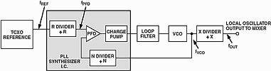
In this configuration, the core PLL is operated at a multiple of the final desired output frequency. In the example given above, the final desired frequency range is 1450 MHz to 1500 MHz. A multiple within the device's frequency range is 5800 MHz to 6000 MHz (four times the desired output band). In the proposed scheme, shown in Figure 4a, ƒPFD operates at 800 kHz, the ƒVCO band is 5800 MHz to 6000 MHz, and the final system LO output is obtained by dividing ƒVCO by four.
Equation 3
ƒOUT = (ƒPFD x N)/X
Some consequences of using this architecture follow.
Phase-noise reduction
The synthesizer phase noise has a 10 log ƒPFD relationship. This means that for every doubling of the PFD frequency, there will be 3 dB degradation in the synthesizer phase noise. However, the output from the VCO will be divided down, and its phase noise obeys a 20 logX rule. So, for every doubling of X, there will be a gain of 6 dB in phase noise performance. If the PFD frequency is quadrupled as above, ƒVCO is divided by four to end up with the correct ƒOUT. Thus 6 dB will be lost due to the quadrupling of ƒPFD and 12 dB is gained due to the division by four. This results in an overall gain of 6 dB in phase-noise performance, using Figure 4a, compared to the use of the standard architecture. In this example, the resulting phase noise would be -94 dBc/Hz.
Reference spur reduction
In an integer-N PLL, spurious frequencies occur at integer multiples of the PFD frequency at the VCO output. In Figure 4a, using ƒVCO, these spurs will be at ƒPFD, 2ƒPFD, 3ƒPFD, etc. However, at ƒOUT, the fundamental frequency is divided by X (X = 4) but the spurious frequencies still exist at the integer multiples of the PFD frequency. Note, however, that they are reduced in amplitude by 20 logX (20 log4 = 12 dB). See Figure 4b.
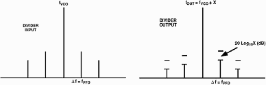
So, using the architecture of Figure 4a with X = 4 and generating an ƒOUT of 1450 MHz to 1500 MHz with 200 kHz spacing, the frequency spurs will exist at integer multiples of 800 kHz, the PFD frequency at levels below -90 dBc. Note that although the step frequency is 200 kHz, the lowest frequency spur is at 800 kHz.
Shorter lock time
Since the PFD in Figure 4a is operating at a higher frequency, phase comparisons are occurring at a higher rate; this will cause the loop to lock faster. In addition, because of the higher PFD frequency, a wider loop bandwidth is possible, and this too helps in improving the lock time. In this example, the lock time is about 70 µs to within 10 degrees of phase error for a PLL loop bandwidth of 80 kHz.
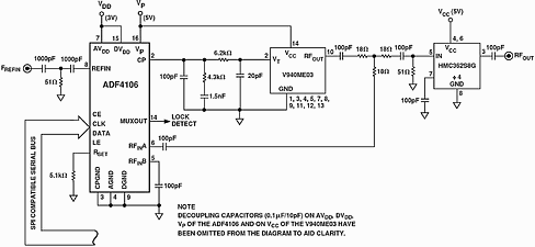
The actual implementation of Figure 4a is shown in Figure 5. To summarise, the circuit of Figure 5 provides the following performance:
* Phase noise: -94 dBc/Hz @ 1 kHz offset
* Reference spurs: <-100 dBc (system noise floor) @ 200 kHz, 400 kHz, 600 kHz offsets; -90 dBc @ 800 kHz offset.
* Lock Time: 70 µs to within 10 degrees phase error.
The price of this improved performance is the extra cost of the output divider and the extra power consumption of the system as a whole (the HMC typically adds 68 mA to the ADF4106's 13 mA current requirement). Thus improved performance must be a critical requirement for selecting this architecture. The extra board space needed for implementation is minimal since the HMC comes in an 8-lead SOIC package.
Bandwidth
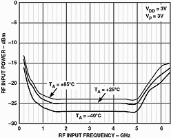
The 0,35 µm BiCMOS fabrication process and careful application of RF design techniques permit the prescaler section of the ADF4106 to operate at up to 6,0 GHz with an input level of -10 dBm (referred to 50 Ohm), guaranteed over the industrial temperature range (-40 to +85°C). Figure 6 shows a typical sensitivity plot for the ADF4106 in a TSSOP package at -40°C, +25°C, and +85°C. It can clearly be seen that performance to 6 GHz is well within the limits of the device with signals below -15 dBm.
Phase noise
Phase noise, a measure of the purity of the local oscillator signal, is the single most critical specification in the local oscillator section of radios - with a direct bearing on receiver sensitivity. It is the ratio to output carrier power of the noise power in a 1 Hz bandwidth at a given offset from the carrier. Expressed as a log ratio, the units of phase noise are dBc/Hz. Phase noise is typically measured with a spectrum analyser.
The circuit of Figure 7 is used as the circuit model for the discussion of phase noise.
Total phase noise in a phase-locked loop (dB) can be expressed as follows:
Equation (1)
PNTOTAL = PNSYNTH + 20logN + 10logƒPFD
where
PNTOTAL is the total phase noise of the PLL
PNSYNTH is the phase noise due to the PLL synthesizer circuit itself
20 logN is the increase of phase noise due to the frequency magnification associated with the feedback ratio, 1/N
10logƒPFD is the increase of noise associated with the incoming PFD frequency
The graph in Figure 8 shows the ADF4106's phase noise characteristics as a function of PFD frequency, ƒPFD. With a given measured total noise, synthesizer noise can be inferred as:
Equation (2)
PNSYNTH = + 20logN + 10 logƒPFD
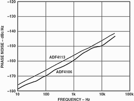
This provides a figure of merit for the PLL synthesizer circuit itself, irrespective of the noise contributed by PLL N value and PFD frequency, since these would be the same for any similar circuit being compared. For the ADF4106, this figure is -219 dBc/Hz, a 3 dB improvement on the ADF4113, which had been the best available integer-N synthesizer in terms of phase noise.
With this phase-noise figure of merit, an engineer can work out the total PLL phase noise for any given PFD frequency and RF output frequency. For example, consider generation of a local oscillator signal with frequencies from 1700 MHz to 1800 MHz and channel spacing of 200 kHz. Using equation (1), the close-in phase noise using the ADF4106 as the PLL synthesizer is
PNTOTAL = -219 + 20 log(9000
+ 10 log(200 x 103)
= -(219 + 79 + 53) dBc/Hz
= -87 dBc/Hz
Figure 8 shows that the ADF4106 obeys the 10 logƒPFD 'rule' (PFD phase noise substantially linear with log frequency) fairly consistently all the way to 30 MHz. Some integer-N devices begin to degrade rapidly once the PFD frequency goes above 1 MHz. Note that the -219 dBc/Hz figure of merit is obtained by extrapolating Figure 8 back to 1 Hz. The graph can be used to quickly identify the performance possible in a given PLL set-up once the N value is known. For example, 200 kHz on the graph corresponds to phase noise of -166 dBc/Hz. Adding 20 logN (79 dBc) gives PLL phase noise of -87 dBc/Hz.
Information provided by Analog Data Products, 011 531 1400, [email protected]


© Technews Publishing (Pty) Ltd | All Rights Reserved
 printer friendly version