


DVB-T (digital video broadcast-terrestrial) decoders will provide a low-cost route into digital TV for the large number of consumers still relying on analog services. A compact, low-cost DVB-T system design with internal AC-DC power conversion can be realised using the features of an integrated power conversion IC from Power Integrations.
Although digital TV continues to offer exciting new features and user benefits, there still remain an estimated 100 million households in Europe that use analog services. To address this market potential, DVB-T-based systems have been developed to offer basic digital TV services. In contrast to the more conventional set-top box, these units are designed to provide basic digital TV through a traditional aerial, in a small, low-cost unit.
The TOPSwitch-GX
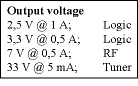
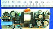
Due to limited space, the power architecture of the first generation decoders has been based on an external AC/DC adapter providing low voltage DC to the unit. This voltage is then converted to the required system rails with internal DC-DC circuitry. It has been estimated that this approach can cost up to 50% more than using a single internal offline converter. By using the advanced features of Power Integrations' TOPSwitch-GX, an offline power supply measuring just 80 x 35 x 16 mm has been realised, allowing for internal offline power conversion and system level cost reduction. A generic specification used is given in Table 1. The prototype has a continuous output power capability of 7,8 W in a 50°C ambient.
In addition to these general requirements, the prototype is designed to meet EN55022 EMI standards with a hard ground on the DVB box output, indicative of functional grounding through a SCART lead. With no hard grounding on the output, EN55022 can be met with a simple pi-filter at the input. In this situation, the common-mode choke and x-cap can be removed, giving further cost and size reduction.
System level benefits
A number of functions integrated into TOPSwitch-GX help to provide excellent system performance and protection without any additional components:
Soft-start reduces current and voltage stress on the primary clamp and output diodes during start-up. Furthermore, output overshoot and transformer saturation effects at start-up are minimised.
Frequency jitter modulates the switching frequency of 132 kHz by approximately ±4 kHz to reduce EMI levels.
Hysteretic thermal protection protects the power supply under output fault conditions. The device will stop switching if the die temperature reaches 140°C (typ). The device will begin to switch again when the die temperature falls below 70°C, ensuring a safe maximum average board temperature of around 105°C during faults.
Auto-restart limits the supply dissipation during a fault on the output such as a short circuit. When the fault is cleared, the supply will automatically resume normal operation.
EcoSmart technology reduces switching frequency under light load conditions to minimise the standby power consumption. On this prototype, a standby power of 330 mW has been achieved.
In addition to these on-chip benefits, the over-voltage protection feature of the chip has been implemented through a 2 MOhm programming resistance (R7 and R8 in Figure 2) from the multifunction pin to the high voltage DC bus. This feature immediately stops device switching when the bus voltage exceeds 450 V d.c. This function will allow the DC bus voltage to transiently reach 700 V without device failure. After the surge has cleared, the device will begin normal switching action again.
Prototype solution
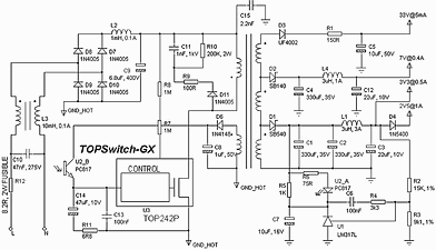
Figure 1 shows the prototype solution centred on a DIL08 version of the TOP242, the smallest GX part. This part occupies minimal board area and requires no external heatsink. Figure 2 shows the prototype schematic. Components C10, L3, L2 and C15 provide filtering of both common-mode and differential mode noise, allowing the EMI regulations to be met even with a hard earth on the output ground. A low-cost RCD snubber has been used for primary side voltage clamping. In order to simplify transformer construction, the 2,5 V output is taken from the 3,3 V line. This could be implemented with an LDO regulator, although a 1N5400 diode was found to provide an adequate voltage drop in the prototype. L4, C12, L1 and C3 form LC post filters on the logic and RF power outputs to give very low noise and ripple. Feedback is provided via a PC817 opto-isolator with an LM317L used as a voltage reference.
Transformer design
The transformer is based on the EF16 core with triple insulated wires for the secondaries. The secondaries are AC stacked to provide good cross-regulation and to minimise the number of pins required on the bobbin. A triple insulated wire design (TIW) has been used to maximise winding width and improve coupling. The winding details are given here:
Primary: 68 turns (930 µH)
Bias: 9 turns
S1: 2 turns
S2: 2 turns in addition to S1
S3: 14 turns in addition to S2
Airgap: 0,1 mm
The bias winding is positioned between primary and secondary to provide an additional shielding function.
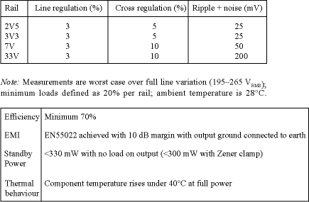
Prototype performance
Performance of the prototype solution was measured in a lab ambient of 28°C with 50 Hz mains from (195 to 265) V r.m.s. The results are given in Figure 3.
Conclusion
DVB-T technology will provide a low-cost route into digital TV for the high number of consumers still reliant on analog TV transmissions. The restricted size of the DVB-T boxes necessitates a highly integrated solution both for the main decoder system and the power provision circuitry. The TOPSwitch-GX based prototype power supply presented offers a high level of system integration and excellent performance with a board area of only 80 x 35 x 16 mm. With the cost of an external supply and internal DC-DC circuitry estimated at 50% higher than a single integrated internal solution, the cost saving over the predicted 100 million DVB-T decoders is highly significant.


© Technews Publishing (Pty) Ltd | All Rights Reserved
 printer friendly version