


Integrated circuits connected to Version 1.1 universal serial Bus (USB) ports are susceptible to damaging electrostatic discharge (ESD) pulses. With frequent overvoltage or over-current occurrences, the conditions exist for soft errors, latent errors or even total system failure.
The modern level of ESD protection within some ICs is 2 kV. This gives protection of the IC/system for normal manufacturing processes nor does it meet the IEC specifications; it does little for the potential ESD environment in modern offices that can generate static voltages very much higher, by merely walking across the floor.
ESD protection devices having moderate capacitive impedances (10 to 100 pF) can be used to shunt the ESD current away from the ICs without distorting the 1,5 or 12 Mbps signals. With the much higher 480 Mbps speed of USB Version 2.0, however, these moderate capacitances will be 480 Mbps.
ESD specifications
USB is a hot insertion and removal specification; it is therefore very vulnerable to ESD as a result of this action. ESD can be induced by air discharge from a number of centimetres away from the USB interface or cable. Therefore, there is universal interest on the part of USB host, hub, and device manufacturers that ESD protection is required. California Micro Devices provides a number of ESD protection devices oriented to USB applications.
ESD requirements
To achieve the higher frequencies of USB 2.0, integrated circuit manufacturers have decreased the minimum dimensions of the transistors, interconnections, and the SiO2 insulation layers. This results in smaller structures that are more susceptible to damage at lower energy levels than when the IC geometries were larger. SiO2 layers are more likely to rupture and metal traces are more likely to open or bridge. The changing environment is also increasing ESD occurrences. There is a proliferation of handheld devices such as cellphones, PDAs, and laptop computers being used in uncontrolled environments (ie, no wrist grounding straps or electrical dissipative/conductive/grounded table surfaces) where people are likely to touch a connector's pin during the connecting and disconnecting of cables.
Some ICs are designed with limited internal ESD protection allowing them to tolerate from 1 to 2 kV pulses (per the human body model standard test), but some ICs are not capable of tolerating even 100 V without suffering damage. Many IC data sheets do not even specify an ESD tolerance voltage, so the user may have to do their own testing to learn what the ESD tolerance is. The generation of ESD charges varies widely with the ambient relative humidity (RH). Walking across a vinyl tile floor with more than 65% RH only generates 250 V of ESD, however if the RH is less than 25%, 12 000 V can be generated.
Picoguard devices
California Micro Device's Picoguard technology uses a diode clamp configuration 1. The process technology to make the diodes, however, is fundamentally different. The Picoguard technology is derived from a metal oxide silicon (MOS) process that is optimised for minimum capacitance. Traditional diode structures are derived from simple bipolar technologies and tend to have higher capacitance levels. The Picoguard technology is the first to combine low capacitance with low voltage clamping levels and high ESD tolerance.
The Picoguard family of ESD protection diodes provides:
* ESD protection of 6 kV per IEC 61000-4-2 (8 kV devices expected in the near future).
* Capacitance of 1,4 pF maximum (1,0 pF typical).
* Low insertion loss (virtually zero up to 2,5 GHz).
* Clamping voltage less than 15 V. (VBUS+10 V) with no higher trigger voltages.
* Sub-nanosecond response time.
* Leakage current of 1,0 µA.
* Small size SOT package.
The low capacitance means the Picoguard device will maintain signal integrity with 480 Mbps USB signals.
Applying the Picoguard ESD protector
Getting maximum protection from any ESD protector requires careful circuit design and layout. While the total ESD energy is not too high, the current waveforms can ramp from zero to ten's of amperes in a nanosecond. Such massive di/dt makes the application extremely sensitive to parasitic inductances. This is because a large voltage drop can occur across a very small inductance since V = L di/dt.
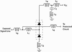
Figure 1 shows the Picoguard circuit in a typical application. All the inductors represent parasitic inductances that might arise from layout configurations.
The effects of these parasitics are:
* Inductors L0, L1 and L6: Inductors L0 and L6 represent the signal line necessary to get from the connector to the internal electronics. L1 arises if the ESD protection device is connected to the main signal line via a stub. This inductance should be minimised and avoided whenever possible as it allows a higher voltage level to be transmitted to the critical device until the back-EMF of L1 can be overcome. Ideally, the signal line should go directly from the external connector to the ESD protection device and from there to the internal electronics with no stubs involved. Also, it is usually best to place the ESD protection device close to the connector, minimising L0, and leaving whatever signal line that is required to get inside the system to act as inductor L6, to shield the internal devices. This also keeps the high ESD voltages and electromagnetic fields created by the ESD current away from other signal lines in the system to avoid possible arcing and/or cross coupling, ie, electromagnetic interference (EMI).
* L5: Inductor L5 represents the inductance from the power pin of the ESD protection circuit to the power supply and to additional bypass capacitors (not shown) that could be used to absorb more of the ESD pulse energy (in addition to C1). This connection to the power supply should always be as direct and as low an inductance as possible.
* C1: A bypass capacitor, C1, should be added to absorb most of the positive ESD pulse. It should be large enough, typically greater than 0,22 µf, to absorb the ESD current without the local supply voltage being significantly increased. This capacitor needs to have very good high frequency characteristics to respond to the fast transition time of the ESD pulse, so ceramic devices are recommended.
* L3 and L4: Inductors L3 and L4 represent the interconnections between the ESD protection device and the bypass capacitor, and from the bypass capacitor to a good ground plane. If these inductances are not small, they will limit the effectiveness of the diode clamp during positive ESD pulses. The lines must be short and wide and C1 should have its ground side tied directly to the ground plane.
* L2: Inductor L2 represents the interconnection from the negative-pulse ESD protection diode to the ground plane. As in the other cases, this line must be as short and as wide as possible to minimise the inductance.
In addition to protecting the USB differential data lines D+ and D-, the VBUS power line should also be protected from ESD pulses. Since the higher capacitance of zener diodes is suitable for the power line, it is recommended that zener diodes be used for this pin. So for two USB ports, a CAMD PACDN042 in a SOT23-2 would be recommended.
Conclusion
The Picoguard ESD protection devices are the most advanced high performance ESD protection devices available. When properly applied, they eliminate system failures caused by ESD pulses while allowing the systems to operate at the high 480 Mbps speeds in USB 2.0 systems.
| Tel: | +27 11 728 4757 |
| Email: | [email protected] |
| www: | www.mbsiliconsystems.co.za |
| Articles: | More information and articles about MB Silicon Systems |


© Technews Publishing (Pty) Ltd | All Rights Reserved
 printer friendly version