


In this article we introduce an alternative receiver design that provides greater flexibility, cost effectiveness as well as providing a means for system upgrades and multilevelled software. This receiver technology is known as multichannel architecture and is possible through recent advances in analog converter technology, which now allow IF sampling which can greatly simplify receiver design. Additional advances in programmable digital integrated tuners simplify filter requirements, allowing their characteristics to be changed through software depending on channel bandwidth and data rates. Together the ADC and digital technology form a chipset that can eliminate many of the cumbersome stages of a traditional analog receiver with predictable and reliable performance and reduce the amount of hardware required for multichannel receivers found in the typical BTS and WLL application.
Using current state-of-the-art ADCs such as the AD6600 and AD6640, IF sampling receivers are a reality. While each of these converters focuses on different receiver applications, they both introduce true IF performance in data converters. The AD6600 is designed for single channel signal processing while the AD6640 is designed for true wide-band, multichannel applications.
While not the only use for such wide-band converters, they are primarily used in multichannel radios such as cellular, PCS and WLL base station receivers. But what level of performance can be achieved and what are the benefits and limitations of such receivers?
Economics of multicarrier receivers
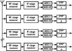
Before an in-depth discussion on performance expectations commences, a few economic comments are in order. In a traditional multichannel receiver design, the receiver is duplicated once for each channel. This produces an overly redundant design. In addition to the duplication of receiver components, the labour to assemble and align these receivers is likewise duplicated.
The real cost of these intangible issues can never be over-estimated. Each added analog stage in a receiver adds expense due to yield, alignment and unpredictability. The sooner the desired signal is digitised, the better. Once digitised, the signal can be tuned, filtered and processed. With this in mind, the following architecture is proposed.
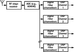
As can be seen, a single RF down-converter followed by a single IF sampling ADC has replaced the multiple front ends. The output of the ADC consisting of the digitised spectral data is then fed to a filter bank consisting of products such as the AD6620 Digital Decimating Receiver.
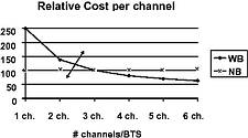
This architecture eliminates the multiple front ends and the cost associated with each of them providing large savings. Thus the incremental cost for each channel then is that only of the digital filter. In the past, the high performance converters demanded a very large premium in cost, but as new converter architectures and silicon processes have been developed, these price premiums have greatly reduced. As shown above, the bulk of all hardware cost in a multichannel receiver is shared between channels. From a recent study of cost models, it can be seen that on a per channel basis, the cost per channel quickly falls below that of a traditional narrow band receiver. Depending on the assumptions made, the crossover point can occur with the first receive channel, especially when IF sampling is performed. Furthermore, as new channels are added to this receiver architecture, the cost per channel falls. That is, when the second channel is added, the receiver per channel cost only half of a typical base band-sampling receiver. These items in brief are the reasons why multichannel receivers can provide a cost advantage. Although this has not been a detailed discussion, it should be evident why this is true.
The full super-heterodyne vs. IF sampling receiver
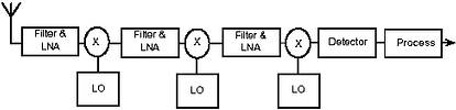
The block diagram of the super-het receiver is shown above. This triple conversion receiver is typical of many designs past and present. Sensitivity is gained by distributing the conversion gain between the antenna and the detector (often times a pair of base-band ADC and DSP). Distributing channel selection through the different stages derives selectivity. Quite often this is done with SAW filters or ceramic filters with specific characteristics determined by the air interface standard of interest. Additionally, most of the conversion gain occurs after the selectivity process begins so those amplifiers with lower IP3s can be used.
Generally, the first local oscillator is variable and responsible for tuning while the second and third is fixed. The fixed local oscillators are usually simple in nature and implemented as crystal oscillators or synthesized with a low cost phased-locked-loop chip and VCO. The variable local oscillator however is another story. Some receiver architectures (such as GSM/DCS- 1800/PCS-1900) require a frequency hopping that must slew and settle in very short order. Therefore, the tunable oscillator demands very close attention.
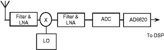
The block diagram of the IF sampling receiver is shown above. This is actually a triple conversion receiver as well but perhaps not visibly so. The first down conversion is the obvious one. The output of the mixer is still an IF signal, possibly up to 90 MHz or so. If the ADC is sampled at 40 MSPS, then the 90 MHz signal is under-sampled and therefore aliased within the ADC. As long as the bandwidth of this signal(s) is less than 20 MHz wide, the Nyquist principle is observed and the signal is aliased (f Signal mod f SampleRate) to base-band without frequency distortion, only translation. Thus aliasing provides the second down conversion. The final down-conversion is provided by the AD6620. This is a digital decimating receiver and designed to down convert the signal to based band. Therefore, it can be seen that this IF sampling receiver is actually still a triple conversion receiver, only the conversions take place through aliasing and numerically through the digital chips.
One difference between these two receiver designs is that with the absence of IF stages, all of the conversion gain must take place prior to the ADC, either in the RF section or in the IF stages after the mixer. This requires that the components selected have a high IP3 since all selectivity is within the digital tuner. This is true because all signal paths, analog and mixed signal, must process the entire spectrum of signals.
Multichannel receivers offer several simplifications. First, the digital chip now replaces the variable local oscillator used for tuning. Thus the analog local oscillator is now fixed, simplifying the design greatly. Second, additional channels can easily be added by the addition of the digital tuner chips, adding greatly to the reliability of the system.
Components required
Of course, to design and build such a receiver takes great consideration in component selection. Several key issues must be addressed. Of course, the issues of noise and intercept point are always of concern when it comes to receiver design, but issues of the data converter must also be discussed. This section will cover many of the components in the receiver.
From our multichannel IF sampling receiver, the first components of concern are the band select filter and LNA. These components are the same as those found in a single channel receiver. This is true because prior to the mixer in a single channel receiver, all signals are present. Therefore, no special points of concern exist with the LNA or filter. Of course, as with any front end, noise figure and IP3 are of great concern since overall noise filter is set by these components.
RF filtering
The RF filter is usually a helical filter. The purpose of this filter is to perform band selection; this is frequently called preselection. In a typical base station, this filter could consist of the bandwidth characteristics of the antenna, the RF trap or coupler (to keep Tx out of the Rx), and the broad band pass filter. As seen later, this filter should exhibit the lowest insertion loss possible, because receiver NF is directly (1 dB per dB) related to insertion loss at the front of the chain. High performance receivers would likely integrate a low loss microstrip filter directly on the PCB to minimise loss in this stage, especially 1800 and 1900 MHz applications. This filter ensures that following stages are not disrupted by any remaining out of band signals, including the base station transmit signals. The filters can be designed specifically to block the transmit side as in TOKO part numbers 6DFSC and 6DFSD.
RF amplifiers and mixers
RF gain stages are available in many forms, including discrete, monolithic and hybrid/MCM technologies. Many manufacturers offer RF front ends suitable for use in many low noise, high intercept applications. Many of these amplifiers offer 13 to 15 dB of gain with noise figures between 1,6 and 3,8 dB with even better performance planned in the future. If ultralow noise figures are required, then discrete transistor amplifiers need be employed.
While large RF gains improve overall noise figure they tend to worsen inter-modulation performance by increasing wide band signal levels to the mixer. Mixers tend to be the most difficult part of the receiver to satisfy.
Low loss mixers (and hence low noise figure) should be used; however, they should have high intercept points. For example, a mixer with a +27 dBm LO drive level typically provides an input intercept point of +37 dBm. Thus, two signals at -43 dBm would give third order inter-modulation (IP3) products at about -200 dBm. However, if the intercept point were lowered to +17 dBm, these products would increase to -163 dBm. As signal levels are increased, inter-modulation performance will reduce rapidly. However, most air interface standards, including GSM and AMPS specification, requires only -43 dBm two tone inter-modulation performance when receiving a reference sensitivity signal. Many mixers in this performance range are available. Since the RF mixer is so near the antenna with so little gain prior, noise is very important. When selecting mixers, it is often tempting to look at active mixers; however, quite often, active mixers have noise figures that are too large. Therefore, the popular choice tends to be the popular diode ring mixers. Since high linearity is required, these are usually the passive diode ring type mixers with high drive levels. These are available from a number of sources, insertion losses for the mixer is typically between 6 and 10 dB.
In addition to the large LO drive levels for optimum performance, these LO signals must exhibit very low phase noise performance. The frequency domain process of the mixer is convolution (the time domain process of the mixer is multiplication). As a result of mixing, phase noise from the LO causes energy from adjacent (and active) channels to be integrated into the desired channel as an increased noise floor. This is called reciprocal mixing.
IF filtering and amplification
Once the signal has been mixed down to an IF that the ADC can handle, the signal must be filtered and then amplified. At this point, the signal must be 'gained' to its full level because once digitised, the signal to noise ratio is fixed (except for process gains, see below). Unlike single channel filtering, a multicarrier radio must pass many channels at the same time. Therefore, the first implication is that the IF filter no longer determines channel bandwidth characteristics. The purpose of the IF filter is to prevent aliasing of unwanted signals by the ADC.
There are two choices for IF filters. The most logical choice for IF filters is a SAW filter because of its relatively low cost. However, since insertion loss is directly proportional to bandwidth, multichannel filters are likely to incur a much higher loss than single channel filters. Where typical single channel losses are perhaps 5 dB, multichannel SAWS may lose up to 25 dB, making post-filtering gain a must. The second option for filtering is the traditional LC filter. While these tend to have phase some phase distortion and cost much more, they do have lower insertion losses, perhaps as little as 3 dB.
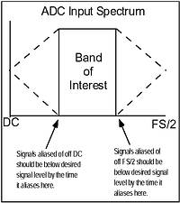
Whether the signals alias off of DC or FS/2, filter skirts need be only as steep as that required preventing unwanted aliasing by the time the filter skirts reach back to the band of interest as shown in the figure above. Thus higher sample rates provide ample opportunity to trade off filter transition bands and unwanted spurious placement.
IF amplification is also a point of concern in a multichannel receiver. Since a multichannel receiver has no selectivity in the analog IF stage, the IF amp has to possess excellent IP3. This stage needs a lot of gain, low noise and very good linearity. If any of these fail to meet the mark, either sensitivity or adjacent channel rejection suffers. Again, looking back at the requirement for AMPS and GSM, two signals around -40's dBm must co-exist without disruption to each other or other channels within the receiver.
Since the gain from the antenna to the mixer is only minimal to prevent mixer overload, the level into the IF amplifier will be very close to that at the antenna port. If two signals at -43 dBm are placed at the antenna, they will be about that same level at the IF amp. Since typical receiver sensitivities are in the general area of about -110 dBm, the inter-modulation products of the IF amplifier must be better than -110 dBm referenced to the IF amplifier input. Thus a quick calculation places the input IP3 of the IF amplifier to be -4,5 dBm. Since amplifier IP3 is normally related to its output, this number must be increased by the gain of the stage. As will be seen later, IF gain requirements range from about 20 to 40 dB. Thus actual IP3 requirements for the IF stage is up to +35 dBm!
In addition to IP3, harmonic suppression can also be important if the IF is actually a base band application. Since this is a multichannel receiver, broad ranges of frequencies are being processed. For example, a GSM receiver would digitise up to 35 MHz, US cellular, up to 25 MHz or US PCS, 5 to 15 MHz. If these frequencies were translated to DC or near DC, then harmonics of these signals would fall back in band. For example, look at US PCS of 5 MHz. If the lowest frequency were translated to 1 MHz, the highest frequency of the band would be at 6 MHz. However, if a carrier were operational at the bottom of the band (1 MHz IF frequency), the second and third harmonic would fall at 2 and 3 MHz respectively, right in the middle of the band. These harmonics definitely can disrupt calls in a wide dynamic such as GSM or AMPS.
Now consider the case where the bottom frequency of the band was translated to 5,1 MHz instead of 1 MHz. The upper frequency would align with 10,1 MHz. Now a quick look at the harmonics shows that the second harmonic of 5,1 MHz would fall at 10,2 MHz, outside the band of interest. The higher the IF frequency, the more spread out the harmonics and signals of interest become. In a practical sense, the IF frequency should be as high as the ADC could reasonably process.
IF amplification
Op-amps are generally out of the question. First they are too noisy and second, they usually do not offer the spurious performance required for IF sampling. This leaves only the use of IF gain blocks. Most of these devices are specified very well down to 5 to 10 MHz, which this application specifies. However, practical IFs will often be around 70 MHz. IF gain blocks are useful in these applications as they offer IP3 specifications as high as +40 dBm. However, when using IF gain blocks, care must be taken to remove the harmonics generated by these devices as they are different than those generated by the ADC. This should not pose a problem.
IF sampling ADC
Recent advances in ADC technology have greatly improved the IF sampling capabilities of analog to digital converters. These improvements are allowing receiver architectures to emerge, primarily IF sampling designs such as those that are the focus of this article. Of those converters, the most current is the AD6640, a 12 bit 65 MSPS converter capable of base band performance up to 80 MHz.
Many of the issues that hold with the IF amplifiers hold true with the ADC as well. The important specifications are harmonic performance and two-tone inter-modulation (a version of IP3). Noise is also an issue, however, the usual design of the analog stage targets analog noise to be above the ADC noise so that it does not fully contribute to the receiver sensitivity.
Digital receiver chip
The purpose of the receiver chip is to tune in the desired carrier and then perform the channel selection of that carrier. Since the chip is fully programmable, the decimation rate and filter characteristics can be changed for each air interface as necessary. Since a typical system will require many receiver chips, it is possible for different air interface standards to be in operation at once. This is possible since each tuner chip can be programmed independent of the others. In this way, one chip can process AMPS and another TDMA or even CDMA.
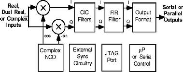
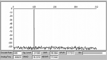
The numerically-controlled oscillator (NCO) provides spurious performance to better than -105 dBc. This ultra clean digital local oscillator is mixed with the digitised input through 18 bit multipliers. As shown in the spectral plot below of the NCO, spurious performance is hidden well in the 16-bit noise floor shown below.
Other than programmable decimation rates, the response of the CIC filters are fixed. The FIR filters are fully programmable and the passband and stop-band characteristics can be programmed to nearly any unique specification.
Inter-stage precision is maintained at 18 bits while individual stages use much higher precision to prevent artifacts due to truncation. Data out of the AD6620 can be delivered to the DSP through either a standard serial interface or through a parallel interface as a memory mapped address device. Data can be delivered in 16, 24 or 32 bit precision.
Possible receiver designs
The next section of this article summarises the performance expectations for a multichannel receiver as proposed here. For more detailed information of evaluating the performance of digital receiver designs, see the ADI applications note titled 'Basics of designing a digital radio receiver'. This outlines many of the considerations when designing a digital receiver and details how to compute receiver sensitivity as shown below. Throughout this section, the AD6640 is the proposed IF sample ADC converter. It should be noted that noise figure is omitted from this discussion. For a complete discussion on receiver design, including noise figure, see the applications note referenced above.
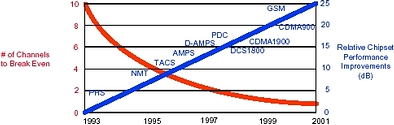
The chart above shows the progression of multichannel multimode receivers. As seen, over the next few years, more and more air interface standards can be implemented with this technology to reduce cost and greatly improve flexibility. In addition, this technology expands into third generation wireless communications as well. Potentially offering very flexible and fully programmable receiver design options.
PHS/PACS
PHS/PACS is a low mobility telephony system, initially deployed in Japan where it is fully deployed. Recently, many providers have begun to turn this into a wireless local loop standard for deployment around the world.
The specifications below are for the PHS system. Referencing the digital receiver block diagram (Figure 2), the following analysis is offered.
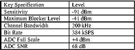
From this table, the maximum allowable conversion gain can be computed.
+4 - (-41) or 45 dB
Allowing for 5 dB of headroom at the top gives 40 dB of conversion gain.
The next question is what sample rate should be used. Since the AD6640 can sample up to 65 MSPS this forms our upper limit. As with all digital standards, the sample rate that is a multiple of the bit rate is the one to use. Since the incoming bit stream must be re-synchronised, we should use four samples per bit. This allows the DSP to determine which of the four samples is actually valid and toss the other three during equalisation. Therefore, the effective bit rate out of the AD6620 must be four times 384 kHz or 1,536 MHz. The first approximation can be found by dividing 65/1,536, which gives 42,317... Using the whole number only, 42 gives a usable sample rate of 42 x 1,536 or 64,512 MSPS. 42 MSPS is also good because it can be easily factored by 2, 3, 6 and 7. A number that can be factored easily is required to distribute the decimation in the AD6620. After a complete filter analysis, the decimation rates used within the AD6620 are 3, 14 and 1. There are several that look good, but this one should minimise internal power dissipation.
The next issue of concern is the processing gain. The actual filter bandwidth as determined from the AD6620 design software is 276 kHz. Therefore, processing gain is:
10 log(64,512/0,276) or 23,7 dB.
Finally the full-scale SNR with process gain is:
68 - 5 (headroom) + 23,7 (process gain) or 86,7 dB
Since 10 dB of SNR is required for minimum detectability for most air interfaces, our signal may be reduced by 77 dB. If an input signal to the receiver of -41 dBm has an SNR of 87 dB, then the minimum detectable signal is:
-41 dBm - 77 dB or -124 dBm
The PHS/PACS spec for minimum signal level is -91 dBm; therefore, this wideband solution can work for PHS/PACS.
CDMA
CDMA air interfaces are becoming very popular for their security and flexibility. CDMA as IS-95 or other future standard offers many advances and features not found in other standards. When implemented using multichannel techniques, multiple standards are possible. As such, one receiver can process AMPS and CDMA at the same time, possibly dynamically allocating spectrum as the demand and user profiles change.
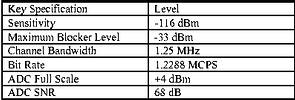
The table above shows the critical operating specification of cellular CDMA (IS-95). From this table, the maximum allowable conversion gain can be computed.
+4 - (-33) or 37 dB
Again allowing for 5 dB of headroom at the top gives 32 dB of conversion gain.
The next issue is how fast to run the sample clock. As with PHS, the AD6640 can sample up to 65 MSPS, however, in the end, we must make sure that our decimated data rate is at least two samples per symbol so that timing/phase recovery can take place. Most CDMA application take four samples per symbol, so even still, interpolation of the output data must take place. Under these conditions, the decimation works out to be (65/(1,2288 x 2)) 26,44. Therefore, the nearest number that has good factors is 24. Therefore, the sample rate will be
1,2288 x 2 x 24 or 58,9824 MHz.
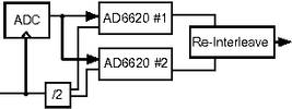
After carefully looking at the design, the decimation rates of two, six and two are selected. This decimation rate provides a total decimation of 24. This design is critical and may only marginally meet the specifications. CDMA requires a decent channel select filter to eliminate the image generated in the digital tuners. CDMA may require extra computing power not available from a single AD6620. In cases such as this, several chips can be paralleled and the required poly-phase filter can be broken up and shared between the two filter chips. The input data to the AD6620 can be decimated between the two chips and the data out of the chips can be re-interleaved for signal processing as shown below.
With these points given, the actual channel bandwidth for our examples is 1,344 MHz. Thus the process gain of our oversampling and filtering can be determined.
10 log(65/1,344) or 16,8 dB
Computing SNR with process gain gives:
68 - 5 (headroom) + 17 (process gain) or 80 dB.
For a CDMA signal, a bank of filters matched to the PN signature sequences of each user, cause each user's signal to be de-spread in frequency, thus affording a further gain in SNR. The spreading scheme described in IS-95 give rise to a processing gain (different from process gain, above) of 128. Assuming completely uncorrelated (or orthogonal) sequences, there is a de-spreading gain of:
10log(128) or 21,07 dB
(1,2288 MHz/9600 baud) is 128
Since 10 dB of SNR is required for minimum detectability and our de-spreading gain is about 21 dB, then our signal can actually be hidden about 10 dB below the noise itself. Thus an actual SNR of -10 dB can recover our signal.
If our signal for 80 dB SNR was -33 dBm, then the minimum detectable signal is:
-33 dBm - 70 -20 dB or -123 dBm
The minimum requirement for CDMA is -116 dBm. Considering that noise figure was ignored, a noise figure of only several dB would render this design useless. Therefore, the cellular CDMA example is a good candidate for a 14-bit converter. However a PCS CDMA implementation would possible make a good solution since the blocking specifications are somewhat reduced.
DCS1800/PCS1900
GSM is deployed worldwide and is one of the most utilised standards around the world. GSM is now being deployed in many parts of the US as PCS1900. This version of GSM is an excellent target for a multichannel receiver technology. These systems have limited bandwidths of 5 to 15 MHz making them well suited for band-pass sampling, placing harmonics out of band.
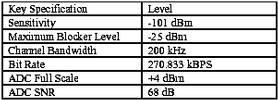
The table above shows the critical specifications for GSM 05.05 as implemented for DCS 1800. As before, this data can be used to calculate the maximum allowable conversion gain.
+4 - (-25) or 29 dB
Allowing for 4 dB of headroom at the top, this gives 25 dB of conversion gain.
The AD6640 can sample up to 65 MSPS. In the end, we must make sure that our decimated data rate is one sample per symbol. One sample per symbol may be used for GSM since the coding scheme is differential. Therefore absolute phase is not as important as which way the vectors have rotated. Therefore, the spectral constellation does not have to have a specific alignment or timing, unlike CDMA or other standards. Since 65 is divisible by 270,833 KBPS, the selected decimation is 240 (65M/270,833K).
Since the bandwidth of the GSM channel is 200 kHz, the digital filter used must provide the bandwidth and shaping required. At any rate the process gain can be computed based on this bandwidth.
10 log(65/0,252) or 24,1 dB.
Finally, full-scale SNR with process gain is:
68 - 4 (headroom) + 24 (process gain) or 88 dB.
Since 10 dB of SNR is required for minimum detectability, our signal may be reduced by 78 dB. If our signal for 88 dB SNR was -25 dBm, then the minimum detectable signal is:
-25 dBm - 78 dB or -103 dBm
The minimum requirement for GSM1800/GSM1900 is -101 dBm; therefore success can be achieved with the Wideband upbanded GSM with a little margin for noise figure. Finally, all of this assumes that dither is used to reduce the spurious performance into the noise floor.
AMPS
AMPS cellular has one of the largest user bases of the air interfaces. It is likely that this standard will persist for many years to come. In order to reduce the cost of future system deployments and to facilitate multimode radios, AMPS is a very likely target for multichannel radios. Along with AMPS, other standards such as NMT are prime candidates for this architecture.
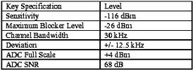
The maximum conversion gain is therefore computed as:
+4 - (-26) or 30 dB
Allowing for 5 dB of headroom at the top gives 25 dB of conversion gain.
Since AMPS is not a digital standard, there is no key sample rate to work with. The main concern will be to sample at a rate that is at least twice the deviation of the signal. However, more importantly, if this is a multimode receiver, then the actual sample rate may be determined by the other standard. However, for the sake of this discussion, the full sample rate of 65 MHz will be used. In the end, the data rate will be four times the deviation or 50 kHz. Thus this gives a decimation rate of 1300 (65M/50k). With this large bandwidth, the FIR filter can utilise a maximum number of taps, giving an excellent filter shape rejecting adjacent channels well.
Since our filter can be well formed, the bandwidth is 30 kHz. Therefore, processing gain is:
10 log(65/0,03) or 33,3 dB.
With process gain at hand, the sensitivity can be calculated:
68 - 5 (headroom) + 33 (process gain) or 96 dB.
Since 10 dB of SNR is required for minimum detectability, the signal may be reduced by 86 dB. If our signal for 96 dB SNR was -26 dBm, then the minimum detectable signal is:
-26 dBm - 86 dB or -112 dBm
The minimum requirement for AMPS is -116 dBm; therefore this fails to meet the requirements of the standard. There are two ways to get around this. The first is to demand a higher resolution ADC, such as 13 or 14 bits. The other solution is to reduce to -26 dBm blocker spec. This would allow more conversion gain and thus better sensitivity. The AMPS spec does not specify this level; it is just a statistical measurement derived by signal measurements at our (ADI's) antenna site. Actually, the closest required specification is that of intermodulation for two signals at about -45 dBm. Therefore, the specification could be relaxed by about 20 dB at the expense of periodic performance degradation if a larger signal overdrives the input to the base station. Therefore, by relaxing the spec to -36 dBm the minimum sensitivity (after an increase in conversion gain) is -123, more than enough to meet the specification.
[Article supplied by Analog Data Products, tel 011 531 1401, [email protected]]


© Technews Publishing (Pty) Ltd | All Rights Reserved
 printer friendly version