


This article will briefly describe the causes, mechanisms, and consequences of latch-up and discuss available prevention methods. Although our aim is to give an understanding of latch-up as it occurs in CMOS switches, similar principles apply to many other CMOS devices.
'Latch-up' may be defined as the creation of a low impedance path between power supply rails as a result of triggering a parasitic device. In this condition, excessive current flow is possible, and a potentially destructive situation exists. After even a very short period of time in this condition, the device in which it occurs can be destroyed or weakened; and potential damage can occur to other components in the system. Latch-up may be caused by a number of triggering factors - including overvoltage spikes or transients, exceeding maximum ratings, and incorrect power sequencing.
Cause
To understand latch-up, we briefly review the basics and understand the participating components. Latch-up occurs as a result of triggering a parasitic device - in effect an SCR (silicon-controlled rectifier), a four-layer pnpn device formed by at least one pnp and at least one npn transistor, connected as shown in Figure 1.
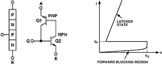
An SCR is a normally off device in a 'blocking state', in which negligible current flows. It behaves similar to a forward-biased diode, but conducts from anode, A, to cathode, K, only if a control signal is applied to the gate, G. In normally-off state, the SCR presents a high impedance path between supplies. When triggered into its conducting state as a result of excitation applied to the gate, the SCR is said to be 'latched'. It enters this state as a result of current from the gate injected into the base of Q2, which causes current flow in the base-emitter junction of Q1. Q1 turns on, causing further current to be injected into base of Q2. This positive feedback condition ensures that both transistors saturate; and the current flowing through each transistor ensures that the other remains in saturation.
When thus latched, and no longer dependent on the trigger source applied to the gate (G), a continual low-impedance path exists between anode and cathode. Since the triggering source need not be constant, it could simply be a spike or a glitch; and removing it will not turn off the SCR. As long as the current through the SCR is sufficiently large, it will remain latched. If, however, the current can be reduced to a point where it falls below a holding-current value, IH, the SCR switches off. Figure 1b shows the current-to-voltage transfer function for an SCR. In order to bring the device out of its conductive state, either the voltage applied across the SCR must be reduced to a value where each transistor turns off, or the current through the SCR must be reduced below its holding current.
A CMOS switch channel effectively consists of PMOS and NMOS devices connected in parallel; control signals to turn it off and on are applied via drivers. Since all these MOS devices are located close together on the die, it is possible that with appropriate excitation, parasitic SCR devices may conduct - a form of behaviour possible with any CMOS circuit. Figure 2 illustrates a simplified cross section showing two CMOS structures, one PMOS and one NMOS; these could be connected together as an inverter or as the switch channel. The parasitic transistors responsible for latch-up behaviour, Q1 (vertical PNP) and Q2 (lateral NPN) are also shown.
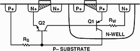
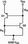
P-substrate is used in devices from the ADG7xx family of switches and multiplexers, while devices from ADG4xx and ADG5xx families use N+ substrate. From Figure 2, it can be seen that a re-interpretation of the silicon configuration shows that the inherent parasitic bipolar transistors, Q1 & Q2, produces the parasitic SCR structure discussed (Figure 3).
Triggering mechanisms
SCR latch-up can occur through one of the following mechanisms.
* Supply voltages exceeding the absolute maximum ratings.
These ratings in the data sheet are an indication of the maximum voltage that can safely be applied to the switch. Anything in excess may result in breakdown of an internal junction and hence damage to the device. In addition, operation of the switch under conditions close to the maximum ratings may degrade long term reliability. It is important to note that these ratings apply at all times, including when the switch is being powered on and off. The triggering mode could result from transients on supply rails.
* Input/output pin voltage exceeding either supply rail by more than a diode drop.
This could occur as a result of a fault on a channel or input - if a part of the system is powered on prior to the supplies being present at the switch (or similar CMOS components in the system). The powered part of the circuit would be sending signals to other devices in the design which may not be able to handle the voltage levels presented. The resulting voltage levels could exceed the maximum rating of the device and possibly result in latch-up. Again, this could occur as a result of spikes or glitches on input or output channels.
* Poorly-managed multiple power supplies.
Switches that have multiple power supplies tend to be more susceptible to latch-up resulting from improper power supply sequencing. Such switches usually have two analog supplies, VDD and VSS, and a digital supply, VL. In some cases, when the digital supply is applied prior to the other supplies, it may be possible for maximum ratings to be exceeded and the device to enter a latch-up state. In general, for those devices that require an external digital supply, VL, we recommend that when power is being applied to and removed from the device, care should be taken to ensure the maximum ratings are not exceeded.
When any of the triggering mechanisms described above occur, the parasitic SCR structure of Figure 1a may begin to conduct, producing a low impedance state between power supply rails. If there is no current limit mechanism on the supplies, excessive current will flow through this SCR structure and through the switch. This could destroy the switch and other components if allowed to persist. With high current levels, a device would not have to remain in a latch-up state for very long; even very brief latch-up can result in permanent damage if current is not limited.
Protection and prevention
But such a fate is not inevitable in CMOS circuitry. The simplest way of preventing latch-up occurring is to adhere to the absolute maximum ratings. If this is not always possible, there are other methods of designing a latch-up-proof system.
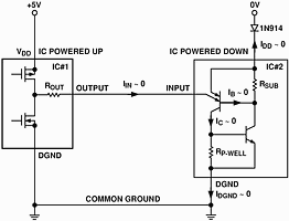
Here are some options for protecting against and preventing latchup: Where it is possible for digital or analog inputs to exceed the VDD supply - either while power is being applied or during operation - the addition of a diode connected in series with VDD prevents base current from flowing, thus avoiding SCR triggering and hence latch-up. While Figure 4 shows the case where the digital input is exceeding the supply of the switch, IC #2, the diode also protects against overvoltages applied to the switch's analog signal path.
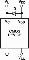
Now, consider a switch with multiple supplies, where for example, the digital supply, VL, may be applied to the device prior to other supplies, exceeding the maximum ratings and exposing the circuit to the potential for latch-up. Internal ESD (electrostatic-discharge) limiting diodes may get turned on, so the simple addition of a Schottky diode, connected between VL and VDD (Figure 5) will adequately prevent SCR conduction and subsequent latch-up. This works very well; it ensures that when VL and VDD are applied to the switch, VDD is always within a diode drop (0,3 V for Schottky) of VL, so the maximum ratings are not exceeded.
Where the addition of an extra component is not a viable option, due to cost or limited board space, switches are available that have been manufactured with a process that ensures that they are latchup-proof. The process uses an insulating oxide layer (trench) between the NMOS and PMOS devices of each switch. This oxide layer is both horizontal and vertical and produces complete isolation between MOS devices, as shown in Figure 6.
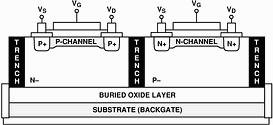
This eliminates the parasitic bipolar devices between transistors, resulting in a latch-up-proof switch. 'Latch-up-proof' means that no matter what way the power is sequenced to the device, latchup cannot occur.
Analog Devices has a number of switches, multiplexers, and channel protectors that have such processing. Although all the devices are latch-up-proof, not all are designed to handle overvoltages outside the supply rails. In addition to these latch-up proof switches, there are other devices that can tolerate under- and overvoltages, with power applied, of +40 V/-25 V in excess of supplies and +55 V/-40 V with power not applied to the device. These devices are specifically designed to ensure that they can handle faults in the event of power-on or -off conditions. They also employ the insulating oxide layer to protect against latch-up. They are available for use either as multiplexers or as channel protectors.
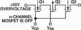
The multiplexers use a structure having n-channel, p-channel, and n-channel MOSFETs in series (Figure 7) to provide both device- and signal-source protection in the event of an overvoltage or power loss. The multiplexer can withstand continuous overvoltage inputs from -40 V to +55 V. When one of the analog inputs or outputs exceeds the power supplies, one of its MOSFETs will switch off, the multiplexer input (or output) appears as an open circuit, and the output is clamped to within the supply rail, thereby preventing the overvoltage from damaging any circuitry following the multiplexer. This protects the multiplexer, the circuitry it drives, and the sensors or signal sources which drive the multiplexer. Figure 7 shows what happens on one channel of the ADG438F in the event of a positive overvoltage. Because the fault protection works regardless of the presence of supplies, the muxes are also ideal for use in applications where power sequencing cannot always be guaranteed to protect analog inputs (eg, hot-insertion rack systems).
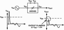
Similarly, channel protectors are used to protect sensitive components from voltage transients in the signal path whether or not the power supplies are present. They are built like the fault-protected muxes described above. When powered, the channel is always in the ON condition, but in the event of a fault, it clamps the output to within the supply rails, as shown in Figure 8.
Channel protectors are generally placed in series with the signal path ahead of standard CMOS processed devices to ensure that potential faults can be tolerated without damage to components in the system. A common way of protecting a channel from potential faults, in either a powered or nonpowered condition, is to connect diodes and current limiting resistors between the channel and the supplies. While it is an effective solution, it requires three extra components per channel, plus the board space to accommodate them. A channel protector would be an equally effective but simpler solution in a single small package.
For example, a channel protector could be used in conjunction with an ADC, switch, multiplexer, or other device to ensure that all the channels are protected, both in the event of an over- or undervoltage, and a fault when the system is unpowered. These devices can withstand continuous voltage inputs from -40 V to +40 V. Because the channel protection works regardless of the presence of supplies, channel protectors are also ideal for use in applications where power sequencing cannot always be guaranteed to protect analog inputs (eg, in hot-insertion rack systems.)
Conclusion
Inasmuch as no application can tolerate latch-up, it is necessary to be aware of its possibility, understand it, protect against it, and take measures to prevent it from happening. Given some thought and the use of available methods and components, it is indeed possible to assemble a latch-up-proof system. While discrete solutions - such as diodes - could be used, devices like latch-up proof switches, fault-protected multiplexers, and channel protectors may provide a simpler, more compact, and more generally suitable solution, resulting in a robust system likely to give fewer problems in the field.
For more information contact Analog Data Products, 011 259 9400


© Technews Publishing (Pty) Ltd | All Rights Reserved
 printer friendly version