


The ability of Synplicity's Certify, Certify SC, and Amplify Physical Optimizer products to automatically convert ASIC-gated clocks to an FPGA-compatible form is a powerful tool for facilitating the prototyping of ASICs in FPGAs.
This short article discusses the use of this feature. It will interest ASIC designers experienced in the design of ASICs using many gated clocks. The ASIC design practice of gated clocks is summarised and contrasted with the FPGA design practice. The article describes the conditions that ASIC gated-clock structures must satisfy in order for Synplicity software to convert them to an FPGA-compatible form.
ASIC gated clocks vs FPGA global clocks
In ASIC designs, gating off clocks to conserve power is a common practice. Typically, an ASIC design is divided into modules, and the clock for a module that is not being used is gated off. In some cases, instead of entirely gating off the clock, the clock frequency is reduced. If current system loading does not require that the module run at full speed, the operating clock frequency of the module can be reduced by clock gating that results in a corresponding savings in power consumption. In a large ASIC design, this practice can result in hundreds of separate clock trees. In ASIC designs, a custom clock tree can be defined for each individual clock tree. When signals cross between different clock trees, the delays at these boundaries are adjusted to ensure that there are no set-up or hold-time violations.
Unfortunately, when prototyping an ASIC design with multiple clock trees into an FPGA, implementing a large number of customised clock trees is not feasible. Creating custom clock trees with unique requirements is a prohibitively difficult task and would require using the FPGA's programmable interconnect. In many cases, the FPGA vendors do not characterise the devices for worst-case minimum delays. In the absence of guaranteed minimum delays, attempting to use static timing analysis to prove that the FPGA does not have any hold-time violations is futile. Also, the FPGA's programmable routing interconnect is a finite resource. Using this resource to implement custom clock trees can lead to routing congestion and potentially an unroutable design.
Overcoming FPGA inability to implement custom clock trees
FPGAs provide a small number of dedicated global clock trees. These clock trees are routed to every sequential device on the die and are designed with such low skew that hold-time violations are guaranteed to be impossible. Using these global clock trees allows the programmable routing resources of the FPGA to be used primarily for logic interconnect and simplifies static timing analysis because checks for hold-time violations based on minimum delays are unnecessary. Placement and routing of the FPGA are likewise expedited. These types of trade-offs and simplifications allow the entire back-end design flow - placement, routing, and successful static timing analysis - for a large FPGA-based design, to be completed in a fraction of the time required to complete the equivalent flow for an ASIC device. Without this time savings, the ability to reprogram an FPGA would be of little advantage. The key to a successful FPGA prototype implementation is to combine most, if not all, of the individual ASIC clocks trees onto the dedicated global clock trees of the FPGA by removing the gating from the clock inputs and moving it to the enable inputs.
Converting gated clocks to FPGA global clock trees
To implement a large number of gated clocks with a much smaller number of global clock trees, the gating is logically separated from the clock and routed to the clock enables on the sequential devices using the programmable routing resources of the FPGA; the ungated or 'base' clock is routed to the clock inputs of the sequential devices using the global clock resources. Because many gated clocks are normally derived from the same base clock, separating the gating from the clock allows a single global clock tree to be used for all of the gated clocks that reference that base clock.
Each sequential device in an FPGA includes a feedback multiplexer controlled by a clock enable as illustrated in Figure 1 of a D flip-flop. The clock enable (CE) input to the feedback multiplexer, when asserted, allows the contents of the flip-flop (the sequential device) to be updated with the D input. When CE is not asserted, the flip-flop retains its value. The feedback multiplexer emulates the functionality of the gated clock.
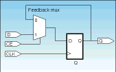
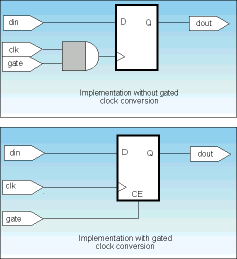
Figure 2 illustrates how a gated-clock implementation is converted to one using clock enable. The RTL implementation with a gated clock is converted to a clock enable implementation in the 'Gated Clock Conversion' view. In this view, the implementation of the feedback mux is not shown. Also, the original base clock, 'clk', connects directly to the clock input of the clock-enabled flip-flop. In an actual design, the clk signal would probably clock many other sequential primitives. Likewise, the gated clock would also clock many other sequential primitives. After the gated clock conversion, all of these sequential primitives would be clocked by the base clock, clk. This base clock would be implemented using the FPGA's global clock which would eliminate clock skew and potential hold-time violations.


© Technews Publishing (Pty) Ltd | All Rights Reserved
 printer friendly version