


Although the move to digital design is providing significant advances in electronics end products, there will always be a portion of circuit design that interfaces with the analog real world. There are some similarities in layout strategies between these two domains, but the differences can make a circuit layout less than optimum. In this article we discuss the fundamental similarities and differences between analog and digital layout with respect to bypass capacitors, power supply and ground layout, voltage errors, and electromagnetic interference (EMI) due to PCB layout.
Similarities of analog and digital layout practices
Bypass or decoupling capacitors - both analog and digital devices require these types of capacitors. In both cases, devices require a capacitor of around 0,1 µF as close to the power pin(s) as possible. Also, a capacitor of about 10 µF is required at the power supply. The positioning of these capacitors is shown in Figure 1. Their values can vary by a factor of around 10, but both must have short leads and be close to the devices or power supply source respectively.
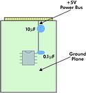
Bypass or decoupling capacitors and their placement on the board are common sense for both types of designs, but interestingly enough, for different reasons. In the analog design, bypass capacitors generally redirect high frequency signals on the power supply that would otherwise enter the sensitive analog chip through the power supply pin. Generally speaking, these high frequency signals occur at frequencies beyond the analog device's rejection capability. The possible consequences of not using a bypass capacitor are the addition of undue noise to the signal path and, worse yet, oscillation.
Decoupling capacitors are also required for digital devices, but for different reasons. One of these is to serve as a 'mini' charge reservoir. A great deal of current is often required in digital circuits to execute the transitions of the changing gate states. Therefore, having additional charge 'on call' is an advantage. The consequence of not having enough charge locally to execute this switching action could be a significant change in the power supply voltage. When the voltage change is too large, it will cause the digital signal level to go into the indeterminate state, probably resulting in erroneous operation of the state machines in the digital device. The switching current passing through the circuit board traces would cause this change in voltage. These traces have parasitic inductance, and the change in voltage can be calculated using the formula:
V = L ΔI/Δt
Where V = voltage change.
L = board trace inductance.
ΔI = change in current through the trace.
Δt = the time it takes for the current to change.
So for a number of reasons, it is a good idea to bypass (decouple) the power supply at the power supply and at the supply pin of active devices.
* The power and ground should be routed together - when power and ground traces are well matched in terms of location, the opportunities for interference are reduced. If they are not matched, the resulting system loops can produce inexplicable 'noisy' results. An example of a PCB designed with the power and ground traces not matched is shown in Figure 2.
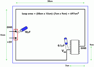
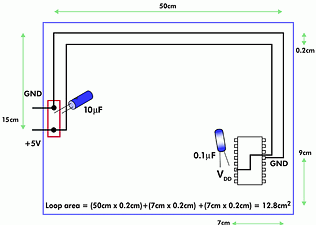
The loop area here is 697 cm2. Induced voltages in the loop, from radiated noise on or off the board, can be reduced dramatically using the approach shown in Figure 3.
Where the domains differ
* Ground planes can be a problem - the fundamentals of circuit board layout apply to both analog and digital circuits. One fundamental rule of thumb is to use uninterrupted ground planes. This common practice reduces the effects of ΔI/Δt in digital circuits, which in turn affects the noise injected into the analog circuits. When mixing digital and analog circuits, the layout techniques are essentially the same, with one important exception. The added precaution that should be taken with mixed-signal circuits is to keep the digital signal lines and return paths in the ground plane as far away from the analog circuitry as possible. This can be done by connecting the analog ground plane separately to the system ground connect or having the analog circuitry at the farthest side of the board, ie, at the end of the line. This ensures that the signal paths receive the minimum amount of interference from external sources. Digital circuitry does not have the same difficulty; it can tolerate a great deal of noise on the ground plane before problems start to appear.
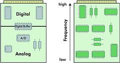
* Location of components - in every PCB design, the noisy and quiet portions of the circuit should be separated as mentioned above. Generally speaking, the digital circuitry is 'rich' with noise and in turn less sensitive to this type of noise (because of the larger voltage noise margins). In contrast, the voltage noise margins of the analog circuitry are much smaller. Of the two domains, the analog domain is most sensitive to switching noise. In the layout of a mixed-signal system, the two domains should be separated - as shown in Figure 4.
* Parasitics designed into the PCB - two fundamental parasitic components - capacitors and inductors - can accidentally be designed into the PCB and cause problems. A capacitor is designed into a board simply by placing two traces close to each other; either on top of each other on two layers or side-by-side on the same layer, as shown in Figure 5. In both configurations, changes in voltage with time (ΔV/Δt) on one trace could generate a current on a second trace. If the second trace is high impedance, this current will convert into a voltage.
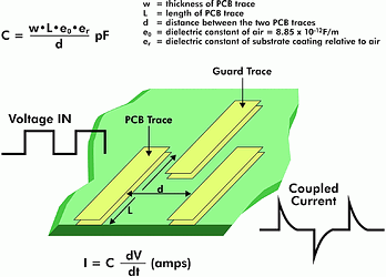
Fast voltage transients are most typically found on the digital side of the mixed signal design. If traces carrying these transients are close to high impedance analog traces, the analog circuitry can be disrupted. This phenomenon can be easily minimised using one of two techniques. The most commonly used is to change the dimensions between the traces as the capacitor equation suggests. The most effective dimension to change is the distance between the two offending traces. As 'd' is increased, the capacitance will decrease. Also, if the length 'L' is reduced the capacitance between the two traces will also be reduced. Another technique is to lay a ground trace between the two offending traces. Not only is the ground trace low impedance, but it will break up the E-fields that are causing the disturbance.
An inductor can be accidentally designed into a board in a similar way to a capacitor, as shown in Figure 6. In both trace configurations, changes in current with time (ΔI/Δt) on one trace could generate a voltage in the second trace and initiate a proportional current. If the voltage change is high enough on the primary trace, the disturbance can reduce the voltage margin of the digital circuitry enough to cause errors. This phenomenon is not necessarily reserved for digital circuits, but is more common in that environment because of the larger, rapidly changing switching currents.
To eliminate potential noise for EMI sources it is best to separate quiet analog lines from noisy I/O ports. Try to implement low impedance power and ground networks, minimise inductance in conductors for digital circuits and minimise capacitive coupling in analog circuits.
Conclusion
When the domains meet, careful layout is critical. Layout strategies usually are presented as rules of thumb because it is difficult to test the success of your final product in a lab environment. So, although there are some similarities in layout strategies between the digital and analog domain, the differences should be recognised.
For more information contact Willem Hijbeek, Tempe Technologies, 011 452 0530, [email protected]
References:
1 Henry W. Ott, Noise Reduction Techniques in Electronic Systems, 2nd ed., Wiley, 1998;
2 Ralph Morrison, Noise and Other Interfering Signals, Wiley and Sons, 1992
| Email: | [email protected] |
| www: | |
| Articles: | More information and articles about Tempe Technologies |


© Technews Publishing (Pty) Ltd | All Rights Reserved
 printer friendly version