

Highly efficient AC-DC power supplies are key to the evolution of the telecom and datacom infrastructure, as power consumption grows rapidly due to hyperscale data centres, enterprise servers, or telecom switching stations. However, the power electronics industry has reached the theoretical limit of silicon MOSFETs.
Meanwhile, recent gallium nitride (GaN) transistors have emerged as a high-performance switch to replace silicon-based MOSFETs, offering increased energy conversion efficiency and enabling greater density. A new isolation concept with new specifications is required to address the advantages of the GaN transistors.
GaN transistors can switch much faster than silicon MOSFETs and can achieve lower switching losses due to:
• Lower gate capacitance and output capacitance.
• Lower drain-source on resistor (RDS(ON)) for higher-current operation, resulting in lower conduction losses.
• Low or zero reverse-recovery charge (QRR), as there is no need for a body diode.
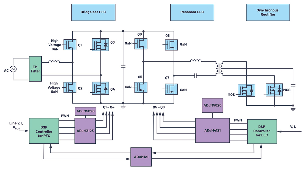
GaN transistors can enable most AC-DC power supplies that consist of separate power factor correction (PFC) and DC-to-DC sections: a front-end, bridgeless PFC and the following LLC resonant converter (two inductors and one capacitor). This topology exclusively relies on half-bridge and full-bridge circuits as shown in Figure 1.
With a digital signal processor (DSP) as the main controller along with the GaN transistor used to replace the silicon MOSFETs, a new isolation technology is required to address the higher switching frequencies. This mainly includes the isolated GaN drivers.
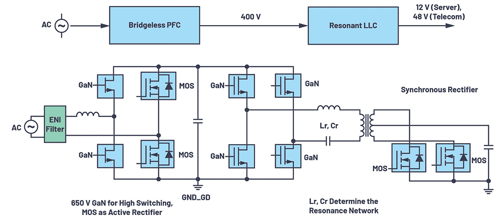 Figure 1. Typical ac/dc power supply for telecom and server applications.
Typical isolation solutions and requirements
UART communication isolation
The change from a previous analog controlled system to a DSP controlled system requires the isolation of the pulse-width modulated (PWM) signals and the additional control signals. The dual-channel ADuM121 can be used for UART communication between DSPs. To minimise the total system size required for the isolation, the epoxy resin sealant is used in board assembly. Smaller size and high power density are critical in the evolution of AC-DC. Smaller package isolators are required.
PFC section isolation
The propagation delay/skew, negative bias/clamp and size of the ISO gate driver are critical for GaN in contrast to MOS. To drive a half-bridge or full-bridge transistor with GaN, the ADuM3123 single-channel driver can be used for the PFC section and the ADuM4223 dual-channel driver for the LLC section.
Powering the devices behind the isolation barrier
Based on Analog Devices’ isoPower technology, which is designed for power transfer across the isolation barrier, the ADuM5020 is a compact chip solution that can match a GaN transistor’s auxiliary power supply with that of a gate.
Isolation requirements
To take full advantage of a GaN transistor, the preferred requirements for isolated gate drivers are:
• Maximum allowable gate voltage <7 V.
• >100 kV/ms dv/dt at switching node, 100 kV/µs to 200 kV/µs CMTI.
• High-low switch delay match ≤50 ns for 650 V application.
• Negative voltage clamp (-3 V) for turning off.
There are several solutions to drive both the high-side and low-side of the half-bridge transistor. One myth about the traditional, level-shifted, high-voltage driver is that the simplest single-chip implementation is widely used only for silicon-based MOSFETs. In some high-end products (for example, power supply for servers), the ADuM4223 dual-isolated driver is used to drive a MOS for compact designs.
However, when turning to GaN, the level-shift solution has disadvantages, such as very large propagation delay and limited common-mode transient immunity (CMTI) and is not optimal for high switching frequency. The dual-isolated driver lacks layout flexibility in comparison to single-channel drivers. Meanwhile, it has difficulty in the configuration of the negative bias. Table 1 shows a comparison of these methods.
Single-channel drivers are ready for GaN transistors. A typical single-channel driver is the ADuM3123, using external power supplied by Zener diodes and discrete circuits for negative bias (optional) as shown in Figure 3.
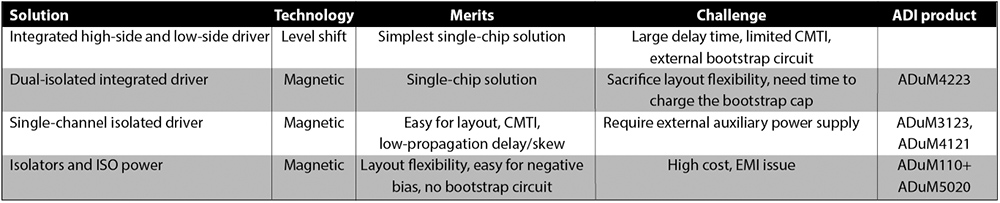 Table 1. Comparison of different methods in driving a GaN half-bridge transistor.
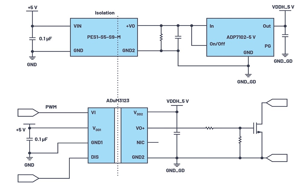 Figure 3. A single-channel, isolated isoCoupler driver application overview for a GaN transistor.
New trend: customised, isolated GaN modules
Presently, GaN devices are typically packaged separately from their driver. This is due to the differences in the manufacturing processes of GaN switches and isolation drivers. In the future, integrating the GaN transistors and the isolation barrier drivers into the same package will further enhance the switching performance as it will reduce the inductor parasitics. Some key telecom vendors plan to package their GaN systems as individual customised modules themselves.
In the long term, the driver for GaN systems may enable its implementation into smaller size isolator modules. Tiny, single-channel examples such as the ADuM110N (low propagation delay, high frequency) and the isoPower ADuM5020, which offer simplicity in design, as shown in Figure 4, support this trend.
 Figure 4. The iCoupler ADuM110N and the isoPower ADuM5020 are good matches for the
Conclusion
GaN transistors with smaller device sizes, lower on-resistance and higher working frequency offer many advantages over traditional silicon-based MOSFETs. Adopting GaN technology could cut total solution size without compromising efficiency. GaN devices have great prospects, especially in medium- and high-voltage power supplies. Analog Devices’ iCoupler technology brings excellent benefits in driving the emerging GaN switches and transistors.
| Tel: | +27 11 923 9600 |
| Email: | [email protected] |
| www: | www.altronarrow.com |
| Articles: | More information and articles about Altron Arrow |






© Technews Publishing (Pty) Ltd | All Rights Reserved
 printer friendly version