29 July 2020Manufacturing / Production Technology, Hardware & Services
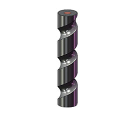
TopLine, represented locally by Test & Rework Solutions, announced that Martin Hart, CEO of TopLine and inventor, has filed for a US patent for a lead-free solder column used in the manufacture of field programmable gate array (FPGA) devices. The unique new product has been developed in anticipation of RoHS requirements for lead-free columns.
In making the announcement, Hart said, “Historically, the aerospace and defence industry has largely been exempt from meeting the requirements of the EU RoHS directive regulating the use of lead in solder columns. It is widely speculated that one day, RoHS will stop renewing its exemption allowing lead-bearing solder balls and solder columns. Doing so could trigger unintentional consequences by forcing original design manufacturers (ODMs) to convert to fully lead-free FPGA products. This product is designed to anticipate and meet future needs for lead-free columns.”
Heritage hardware used in the aerospace and defence industries are built on a platform of FPGA devices built with solder columns instead of solder balls, Hart adds. Column grid array (CGA) FPGA packages engaged in mission-critical black box systems have shown to be more reliable than ball grid array (BGA) packages, absorbing stress and increasing solder joint reliability under harsh operating conditions.
200 W of power in a space-saving design Vepac Electronics
Manufacturing / Production Technology, Hardware & Services
The Hakko FX-972 Soldering Station delivers high-performance soldering in a compact package, making it suitable for a wide range of soldering applications.
Read more...FineX: Makes shielding clear Avnet Abacus
Manufacturing / Production Technology, Hardware & Services
Panasonic Industry launches high-transparency, low-resistance, flexible transparent conductive film for electromagnetic wave shield with pre-applied OCA.
Read more...Collaboration is now critical RS South Africa
Manufacturing / Production Technology, Hardware & Services
The message emerging from RS Connect is clear: Organisations can no longer rely on internal optimisation alone to secure performance. Competitive advantage is increasingly being determined by the strength of external relationships, shared capability and coordinated action across value chains.
Read more...Disruption is the new normal. Effortless is the new competitive advantage. Seven Labs Technology
Manufacturing / Production Technology, Hardware & Services
Global supply chains have been under pressure for years. The manufacturers still standing are the ones who stopped waiting for normal to return, and started building something better.
Read more...World-first 016008 mm component placement
Manufacturing / Production Technology, Hardware & Services
Fuji has achieved the world’s first placement of 016008 mm (0,16 x 0,08 mm or 006 x 003 inches) size components on printed circuit boards with its SMT pick and place machine, NXTR.
Read more...Lifecycle and obsolescence: Protecting electronics through process Production Logix
Manufacturing / Production Technology, Hardware & Services
At Production Logix, we believe longevity is not accidental. It is engineered through early visibility, structured response, and disciplined execution, in partnership with our OEM customers.
Read more...Maximising squeegee quality and durability Testerion
Manufacturing / Production Technology, Hardware & Services
Transition Automation has announced two new product advancements designed to improve SMT printing performance and extend squeegee life: laser-enhanced Permalex bonding and integrated edge protectors.
Read more...NeoDen ND2 PCB screen printer ZETECH ONE
Manufacturing / Production Technology, Hardware & Services
The NeoDen ND2 PCB screen printing machine is a fully automatic stencil printer designed to deliver precise and consistent solder paste application in modern SMT production environments.
Read more...Understanding the BGA rework process Techmet
Manufacturing / Production Technology, Hardware & Services
BGA rework is a highly technical process that involves removing the faulty component, preparing the circuit board, and installing a new or repaired device, while maintaining the integrity of the printed circuit board.
Read more...Flexible three-process reflow soldering system Truth Electronic Manufacturing
Manufacturing / Production Technology, Hardware & Services
By combining multiple soldering technologies within a single system, the Vision TripleX system enables manufacturers to adapt easily to different assembly requirements, board designs, and production volumes.
While every effort has been made to ensure the accuracy of the information contained herein, the publisher and its agents cannot be held responsible for any errors contained, or any loss incurred as a result. Articles published do not necessarily reflect the views of the publishers. The editor reserves the right to alter or cut copy. Articles submitted are deemed to have been cleared for publication. Advertisements and company contact details are published as provided by the advertiser. Technews Publishing (Pty) Ltd cannot be held responsible for the accuracy or veracity of supplied material.


 printer friendly version