31 August 2022Manufacturing / Production Technology, Hardware & Services
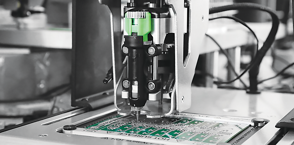
Have you ever wished for a quick solution to prototyping electronic circuit boards? If you have, then the Voltera V-One, a multi-functional circuit board printer, may be just what you need.
The V-One is an all-in-one solution for PCB fabrication that allows you to keep your development cycle secure, thereby keeping your intellectual property completely in-house. The printer allows for rapid prototyping of circuit board layouts by combining the following four functions: printing traces of conductive ink onto substrate, drilling through-holes and vias on the board, precisely dispensing solder paste, and reflowing components using the built-in heating plate.
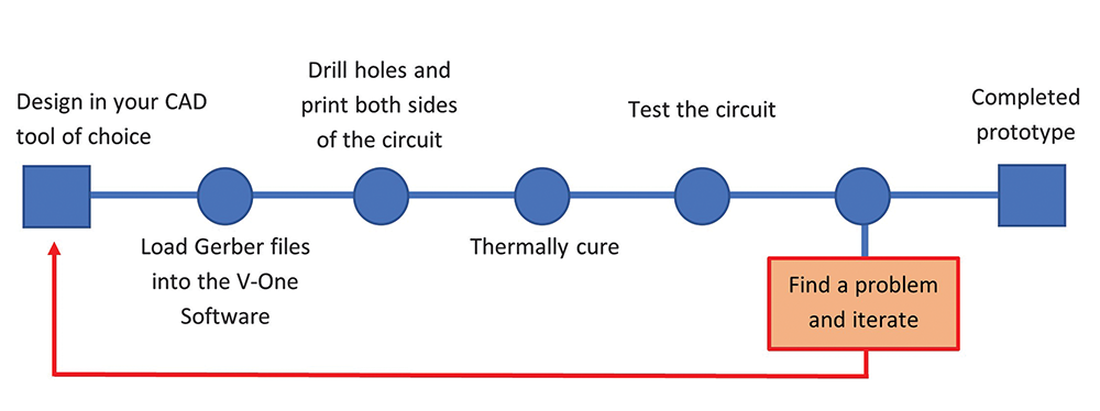
From the initial idea through to the finished board, the V-One makes prototyping a cinch. The electronic board layout is designed in the software of one’s choice and the Gerber files are uploaded to the V-One software. Once the printer has been calibrated, holes and vias are drilled on both sides of the board together with the printed tracks, and the board is then thermally cured. Solder paste is then applied to the board and the components are inserted via the newly drilled holes. The printer then provides component reflow to produce the completed prototype.
The electronic circuit can then be tested and should a problem be found, a new board with the correction can be printed, thereby providing a rapid turnaround time and theoretically shaving weeks off a product development cycle. Teams at top companies worldwide are already using the V-One for rapid prototyping of electronic designs.
The V-One software, combined with Voltera’s smart height probe, allows for precise alignment of the print and drill heads. The drill head, although compact, is capable of drilling through-holes and vias at 13 000 rpm with a runout of only 3 mil. Once drilling is completed, the dispense nozzle deposits ink or solder paste on boards with a 0,65 mm pin-to-pin pitch, allowing for precise circuit tracks to be laid down. Finally, the unit cures the ink and provides reflow and, together with the pre-defined heating profiles and the 550 W heating element, allows for the print bed to reach a temperature of 240°C.
The printer’s software application is completely free of charge and provides an intuitive interface to all functions necessary to produce a finished prototype PCB. The application contains smart alerts when designing the layout, to prevent printing issues, and step-by-step video instructions walk the user through the different stages of the production process.
The V-One’s small dimensions of only 390 x 257 x 207 mm and modern look allows it to seem at home in any environment: on an office desk, a laboratory table, or on a workshop bench.
World-first 016008 mm component placement
Manufacturing / Production Technology, Hardware & Services
Fuji has achieved the world’s first placement of 016008 mm (0,16 x 0,08 mm or 006 x 003 inches) size components on printed circuit boards with its SMT pick and place machine, NXTR.
Read more...Lifecycle and obsolescence: Protecting electronics through process Production Logix
Manufacturing / Production Technology, Hardware & Services
At Production Logix, we believe longevity is not accidental. It is engineered through early visibility, structured response, and disciplined execution, in partnership with our OEM customers.
Read more...Maximising squeegee quality and durability Testerion
Manufacturing / Production Technology, Hardware & Services
Transition Automation has announced two new product advancements designed to improve SMT printing performance and extend squeegee life: laser-enhanced Permalex bonding and integrated edge protectors.
Read more...NeoDen ND2 PCB screen printer ZETECH ONE
Manufacturing / Production Technology, Hardware & Services
The NeoDen ND2 PCB screen printing machine is a fully automatic stencil printer designed to deliver precise and consistent solder paste application in modern SMT production environments.
Read more...Understanding the BGA rework process Techmet
Manufacturing / Production Technology, Hardware & Services
BGA rework is a highly technical process that involves removing the faulty component, preparing the circuit board, and installing a new or repaired device, while maintaining the integrity of the printed circuit board.
Read more...Flexible three-process reflow soldering system Truth Electronic Manufacturing
Manufacturing / Production Technology, Hardware & Services
By combining multiple soldering technologies within a single system, the Vision TripleX system enables manufacturers to adapt easily to different assembly requirements, board designs, and production volumes.
Read more...Inline vapour phase soldering for high-volume production MyKay Tronics
Manufacturing / Production Technology, Hardware & Services
The VP2200-100 vacuum inline vapour phase soldering system from ASSCON is designed for fully automated, high-volume electronics manufacturing where process consistency and solder joint quality are critical.
Read more...Global electronics solutions since 1964 IMP Electronics Solutions
Manufacturing / Production Technology, Hardware & Services
Over more than six decades, IMP Electronics Solutions has built a reputation for technical expertise, reliable supply chains, and strong partnerships with both customers and manufacturing partners.
Read more...Driving excellence in electronics manufacturing Jemstech
Editor's Choice Manufacturing / Production Technology, Hardware & Services
Jemstech’s reputation for disciplined execution and client-focused service has earned it strong loyalty from companies operating in demanding industries.
Read more...When do you need Nitrogen in reflow? Truth Electronic Manufacturing
Manufacturing / Production Technology, Hardware & Services
Nitrogen in reflow soldering is often seen as a performance enhancer, offering improved wetting, shinier joints, and fewer defects. But it is not always necessary.
While every effort has been made to ensure the accuracy of the information contained herein, the publisher and its agents cannot be held responsible for any errors contained, or any loss incurred as a result. Articles published do not necessarily reflect the views of the publishers. The editor reserves the right to alter or cut copy. Articles submitted are deemed to have been cleared for publication. Advertisements and company contact details are published as provided by the advertiser. Technews Publishing (Pty) Ltd cannot be held responsible for the accuracy or veracity of supplied material.


 printer friendly version