28 June 2023Manufacturing / Production Technology, Hardware & Services
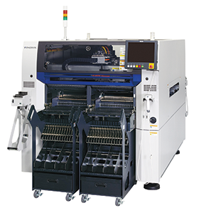
Yamaha Motor Europe Robotics SMT Section has announced a new YRM20DL surface mounter.The YRM20DL is a premium high-efficiency modular design that achieves improved actual and per-unit-area productivity, with a newly developed high-rigidity dual-lane conveyor, further reducing transport losses. The YRM20DL is built on the basic performance of the company’s flagship high-speed, high-accuracy, high-versatility, universal mounter YRM20.
The YRM20DL supports a maximum PCB width of up to 330 mm, where the same width PCB is being conveyed at the front and rear while in dual-lane production mode. In the case of parallel mounting, the front and rear heads can operate without any interference up to a maximum PCB length of 380 mm, enabling high-efficiency mounting without loss.
The basic performance of the unit has been further enhanced to achieve a productivity of up to 120 000 CPH, along with a higher-accuracy placement of ±15 µm (Cpk ≥ 1,0) through the revision of the layout such as bringing the mounted components pick-up area and the mounting area closer together, optimising the main spindle motion control, and improving the rigidity of the conveyor. The RM head/HM head supports 0201 (0,25 x 0,125 mm) sized ultra-small chip component mounting and narrow adjacent mounting.
The newly developed high-rigidity dual-lane conveyor supports a maximum PCB width of up to 330 mm where the same width PCB is being conveyed at the front and rear while in dual-lane production mode. An ultra-high-speed rotary RM head that employs overdrive motion (mutual head insertion) allows the front and rear heads to operate without any interference up to a maximum PCB length of 380 mm, enabling highly efficient mounting without head standby loss.
In single-lane production, which uses only one of the two lanes, it is possible to transport PCBs up to a maximum length of 810 mm, a maximum width of 610 mm, a transportable weight of 3 kg, and a maximum PCB thickness of up to 6,5 mm. This new model is also compatible with a wide range of extra-large-sized PCBs, including for automotive products, industrial, medical, power devices, and LED lighting.
World-first 016008 mm component placement
Manufacturing / Production Technology, Hardware & Services
Fuji has achieved the world’s first placement of 016008 mm (0,16 x 0,08 mm or 006 x 003 inches) size components on printed circuit boards with its SMT pick and place machine, NXTR.
Read more...Lifecycle and obsolescence: Protecting electronics through process Production Logix
Manufacturing / Production Technology, Hardware & Services
At Production Logix, we believe longevity is not accidental. It is engineered through early visibility, structured response, and disciplined execution, in partnership with our OEM customers.
Read more...Maximising squeegee quality and durability Testerion
Manufacturing / Production Technology, Hardware & Services
Transition Automation has announced two new product advancements designed to improve SMT printing performance and extend squeegee life: laser-enhanced Permalex bonding and integrated edge protectors.
Read more...NeoDen ND2 PCB screen printer ZETECH ONE
Manufacturing / Production Technology, Hardware & Services
The NeoDen ND2 PCB screen printing machine is a fully automatic stencil printer designed to deliver precise and consistent solder paste application in modern SMT production environments.
Read more...Understanding the BGA rework process Techmet
Manufacturing / Production Technology, Hardware & Services
BGA rework is a highly technical process that involves removing the faulty component, preparing the circuit board, and installing a new or repaired device, while maintaining the integrity of the printed circuit board.
Read more...Flexible three-process reflow soldering system Truth Electronic Manufacturing
Manufacturing / Production Technology, Hardware & Services
By combining multiple soldering technologies within a single system, the Vision TripleX system enables manufacturers to adapt easily to different assembly requirements, board designs, and production volumes.
Read more...Inline vapour phase soldering for high-volume production MyKay Tronics
Manufacturing / Production Technology, Hardware & Services
The VP2200-100 vacuum inline vapour phase soldering system from ASSCON is designed for fully automated, high-volume electronics manufacturing where process consistency and solder joint quality are critical.
Read more...Global electronics solutions since 1964 IMP Electronics Solutions
Manufacturing / Production Technology, Hardware & Services
Over more than six decades, IMP Electronics Solutions has built a reputation for technical expertise, reliable supply chains, and strong partnerships with both customers and manufacturing partners.
Read more...Driving excellence in electronics manufacturing Jemstech
Editor's Choice Manufacturing / Production Technology, Hardware & Services
Jemstech’s reputation for disciplined execution and client-focused service has earned it strong loyalty from companies operating in demanding industries.
Read more...When do you need Nitrogen in reflow? Truth Electronic Manufacturing
Manufacturing / Production Technology, Hardware & Services
Nitrogen in reflow soldering is often seen as a performance enhancer, offering improved wetting, shinier joints, and fewer defects. But it is not always necessary.
While every effort has been made to ensure the accuracy of the information contained herein, the publisher and its agents cannot be held responsible for any errors contained, or any loss incurred as a result. Articles published do not necessarily reflect the views of the publishers. The editor reserves the right to alter or cut copy. Articles submitted are deemed to have been cleared for publication. Advertisements and company contact details are published as provided by the advertiser. Technews Publishing (Pty) Ltd cannot be held responsible for the accuracy or veracity of supplied material.


 printer friendly version