


When considering the long-term reliability of integrated circuits, a common misconception is that high package or die thermal resistance is problematic. However, high or low thermal resistance, by itself, tells an incomplete story.
More important is how power dissipation combines with thermal resistance to increase the temperature of the die junction along with the maximum rated operating temperature of the die junction. The operating temperature of the die, commonly referred to as the junction temperature for bipolar junction transistors (BJTs) and the channel temperature for field effect transistors (FETs), directly affects the device mean time to failure (MTTF).
This application note explores this topic and provides simple equations that establish how power consumption and thermal resistance affect die junction temperature and reliability. The article particularly focuses on gallium arsenide (GaAs) and gallium nitride (GaN) RF amplifiers in lead frame chip scale packages (LFCSPs).
A typical LFCSP
Figure 1 shows the side profile of a typical LFCSP mounted on a multilayer PCB. The LFCSP consists of a GaAs, GaN, or silicon die sitting on a metal pad that is soldered to the PCB. Bond wires, which are encased in the plastic overmold, connect the die pads to the device pins (See figure 1).
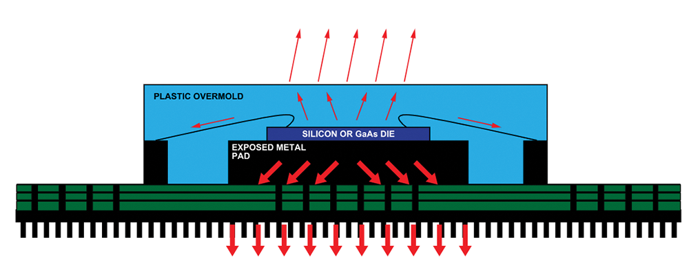 Figure 1. Side profile of a typical LFCSP.
The path of lowest thermal resistance from the die is through the exposed metal pad and into the PCB. The PCB normally has vias that conduct heat to the underside of the board where a heatsink may be attached. While some heat flows through the plastic to the top of the package and through the bond wires, the majority of the heat dissipates through the exposed pad (indicated by the large red arrows in Figure 1).
Thermal resistance from junction to case (θJC) is a metric of how easily heat flows from the die junction to the exposed pad (note that while FET devices have channels rather than junctions, the term junction-to-case is widely used to express the thermal resistance of both BJT and FET devices).
The unit of thermal resistance is °C/W, and it typically ranges from 2°C/W to 150°C/W. If the thermal resistance is known, the temperature of the die junction can be calculated based on the temperature of the exposed pad and the power consumption.
TJ = TCASE + (Power Consumption × Thermal Resistance) [1]
where Power Consumption is the power consumed inside the package.
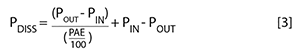
PDISS = PIN + (VDD × IDD) - POUT [2]
Equation 2 can also be written using power added efficiency (PAE).
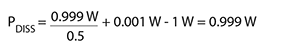
For example, if input power and output power are 1 mW and 1 W, respectively, and the PAE is 50%:
Once the power dissipation inside the package is known, the temperature of the die junction can be calculated using equation 4:
TJ = Case Temperature + (Thermal Resistance × Power Dissipation) [4]
For example, if the case temperature is 85°C and the thermal resistance is 10°C/W, the die junction temperature from the previous example is:
TJ = 85°C + (10°C/W × 0.999 W) = 94.99°C
MTTF is calculated based on the results of high temperature life testing and is generally specified at 85°C die junction temperature. MTTF can be recalculated if the device is expected to spend most of its lifetime operating at a lower or higher temperature.
Focusing on die junction temperature
As already discussed, die junction temperature is a function of case temperature, power consumption, and thermal resistance. Consider the following two cases. A GaAs power amplifier consumes 10 W of power and has a junction-to-case thermal resistance of 5°C/W. If the case temperature is 85°C, the die junction temperature is 135°C.
Next, consider a low noise amplifier with internal power consumption of 500 mW and thermal resistance of 100°C/W. When its case temperature is at 85°C, the die junction temperature is also 135°C. Both devices are operating 40°C below their maximum specified junction temperature of 175°C.
All other things being equal, the two devices have similar MTTF and life expectancy. The key point is that high thermal resistance is not necessarily a bad thing. It must be viewed in the context with the typical power consumption of the device. It is the die junction temperature that is most critical.
Why do lower power amplifiers sometimes have much higher thermal resistance compared to higher power devices? RF power amplifiers must be designed to have low thermal impedance (typically 1°C/W to 15°C/W). Without low thermal resistance, die junction temperatures of these devices run too hot and exceed the absolute maximum rating of the semiconductor process.
When lower power amplifiers are being developed, the IC designer is not bound by the same thermal limitations. They can focus on optimising RF performance, while ensuring that the die junction temperature is kept to a reasonable level. If necessary, they can trade off thermal resistance against die size and device performance.
| Tel: | +27 11 923 9600 |
| Email: | [email protected] |
| www: | www.altronarrow.com |
| Articles: | More information and articles about Altron Arrow |


© Technews Publishing (Pty) Ltd | All Rights Reserved
 printer friendly version