


Insituware integrates hardware and software technology to enable the rapid assessment of materials during use. It combines advanced analytical sensors, smart devices, and intelligent cloud-based information with innovative packaging methods to enable nonintrusive sensing of materials in motion. The company is a subsidiary of Systems Innovation Engineering (SIE), an innovative technology-driven company that provides systems engineering capabilities specifically designed to improve supplier resiliency and overall product affordability.
“Insituware revolutionises the way we control materials in manufacturing, sense physiological changes in sports, understand materials performance in aviation, and measure critical changes in construction materials,” according to Insituware co-founder, David Tafuna.
Insituware is cloud-based and operates with a local family of materials-specific apps on a handheld device. It integrates technology that enables better control of materials by performing rapid assessments of materials on location and during use or in situ, meaning ‘in place’. With a combination of advanced analytical sensors, smart devices, and intelligent cloud-based information with innovative packaging methods, Insituware enables nonintrusive sensing.
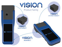
Insituware Vision product family
The Insituware Vision product family consists of the MARK-1 handheld device, the plug-and-play Insight modules, material specific MARK-1 application programs (apps), and the Insitucloud which incorporates the data management system, MethodQC (the statistical process control software), and the machine learning back-end analysis system. The Vision product family operates seamlessly to enable rapid and intelligent measurements in the factory while trending and tracking the collected data from any computer with Internet access.
The initial implementation of the Vision product family is in the electronics manufacturing space – enabling the monitoring and control of laminates, soldering materials, coatings, masks, and adhesives. This family of products will also enable the characterisation and identification of residues to assure effective cleaning processes and ultimate product reliability.
Vision MARK-1 and Insight modules
The Vision MARK-1 handheld device with associated plug-and-play Insight modules expand the functionality of the Vision MARK-1 device to enable the non-destructive inspection and process control of a variety of materials both before and during use.
Insituware apps
The touch of a button on the Vision MARK-1 shows results that can increase efficiency, knowledge and productivity. Insituware’s hardware device technology is designed to be used as a partner with materials-specific Insituware apps, allowing users to see and use customisable results to better monitor and control materials.
The Insituware apps, combined with Vision MARK-1, are infused with smart in-situ technology that integrate statistical process control analysis methods (MethodQC) and machine learning in a cloud environment.
Insitucloud
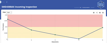
The Insitucloud with MethodQC expands the reach of an Insituware device by providing access to a repository of materials data. By using the Insitucloud, users can rapidly identify unknown materials, investigate global and local changes in materials, and identify the root cause of material degradation or failure. The Insitucloud continuously improves to provide users with state-of-the-art materials knowledge and predictive models to make informed decisions.
Insituware’s focus is to build platforms, not just products, making it solutions-focused as opposed to sensors-focused. It accomplishes this goal by measuring materials in situ (i.e., while in use) to allow for rapid decision making. Measurements in situ provide numerous benefits over lab measurements. While measurements in a lab are accurate, they are also expensive and slow, requiring trained lab technicians and costly equipment as well as the time to ship materials to the lab facility.
Benefits of measuring materials while in use prove to be:
• Effective: Enables users to make decisions quickly.
• Inexpensive: Highly integrated analytical sensors can be deployed at scale.
• Quick: Automated interpretations generated using machine learning methods.
Insituware team members make it a priority to help customers measure in situ. First, they use the latest generation of integrated, miniaturised analytical sensors. Next, they perform data science and machine learning techniques to compensate for the in-field sensor outputs. This helps customers replace a trained technician with automated software. Finally, they connect all sensors to a centralised cloud backend to enable big data analyses. This gathers and stores sensor data to continually improve the system.
Tafuna adds, “It is important to be solutions-focused, rather than sensor-focused. Many IoT companies start at the sensor and try and find use cases. We start at the problem and find the best sensors to solve the problem.” Starting with the sensor and attempting to create relevant applications can result in companies that are siloed and force a solution to a problem. Tafuna says that innovative solutions are created when designing products with an in-depth understanding of the material being measured.
In the same vein, Insituware builds platforms, rather than just products, because this approach enables reuse and significantly speeds development. Careful architecture allows for reuse at multiple levels. A range of materials can be measured, making Insituware a viable, important solution over a range of industries:
Metals: Insituware measures the presence of oxides on the surface of metals and associated reactions between these oxides and other materials. Understanding surface oxide properties is critical in many metals’ surface preparation, processing and soldering activities. Additionally, the presence of oxides and reaction products on certain metals provides an indication of an environmental corrosion process occurring.
Polymers: Insituware detects the consistency of a post-cured polymer, measures the cure state of polymers, and predicts post-cure behaviour of polymers while in the pre-cure state. Understanding the consistency and cure state of polymers helps understand their mechanical and hygroscopic properties. Being able to predict the post-cure state of a polymer prior to use can save significant cost in processing materials and repair.
Biomaterial: Athletes in the field, on stage or otherwise are continuously driving for peak physical performance that only comes through years of conditioning and overload training. Understanding physiological changes during this conditioning process optimises performance improvement and reduces the probability of injury. Insituware noninvasively senses and evaluates physiological materials during this conditioning process, whether it be through exercise, training or other physical activities.
Tafuna concludes, “Real-time intelligent solutions enable rapid decisions.” Insituware’s ability to quickly assess materials during use opens a new dimension of measurement. Combining sensors, smart devices and intelligent cloud-based information with packaging allows for new ways to control materials in manufacturing, sense changes in sports, and understand materials performance in aviation and construction.
| Tel: | +27 11 824 1427 |
| Email: | [email protected] |
| www: | www.techmet.co.za |
| Articles: | More information and articles about Techmet |


© Technews Publishing (Pty) Ltd | All Rights Reserved
 printer friendly version