31 July 2024Manufacturing / Production Technology, Hardware & Services
Pursuing higher speeds in production and manufacturing requires a wide range of up-to-date technologies, ranging from hardware design to development of the image processing software. Optimising parts such as cameras and processed image data, and coordinating each component’s operation, are vital to a correctly functioning high-speed system.
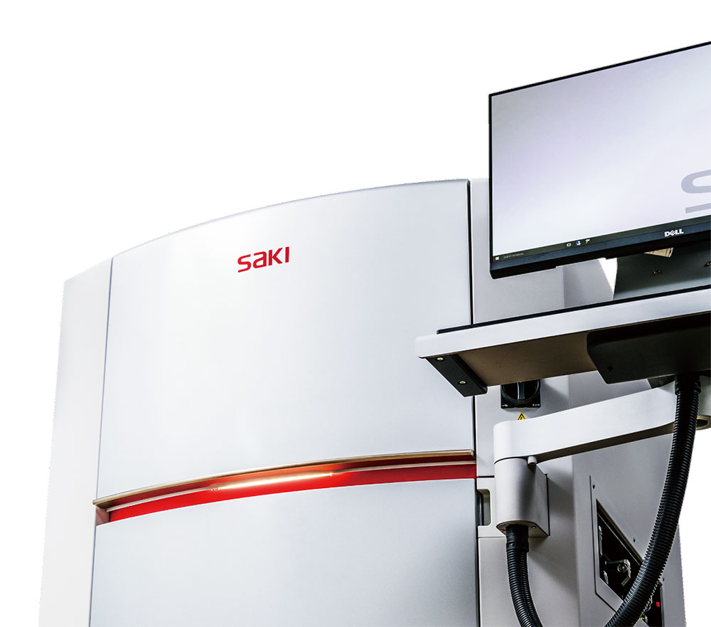
Saki develops all products and key technologies in-house, allowing for the extensive optimisation of hardware and software of their automated optical inspection (AOI) systems.
The company’s latest AOI and AXI (automated X-ray inspection) has an expanded field of view size allowing for imaging with a smaller field of view. This allows an optimised optical system to achieve 4500 mm2/s with the 8 µm camera, and 7000 mm2/s using the 15 µm camera. With optimisation of both the wide-area imaging detector and image processing, AXI machines have reduced takt time by up to 50% compared to the previous model.
Saki’s solutions have also been upgraded to incorporate a highly stable biaxial structure for the camera gantry. Combined with the ultra-rigid frame and fully closed-loop motor drive, this ensures exceptional stopping position accuracy. This hardware structure allows high-definition images to be captured, even when the optical head is moved at high speeds.
The custom software developed in-house provides advanced image processing from basic imaging to 3D image rendering. Processing is performed alongside imaging to speed up cycle times and reduce unnecessary waiting time. Both AOI and SPI use the same software, and the AXI rendering of 3D images and CT calculations for X-rays also benefit from the software developed in-house for full hardware integration.
200 W of power in a space-saving design Vepac Electronics
Manufacturing / Production Technology, Hardware & Services
The Hakko FX-972 Soldering Station delivers high-performance soldering in a compact package, making it suitable for a wide range of soldering applications.
Read more...FineX: Makes shielding clear Avnet Abacus
Manufacturing / Production Technology, Hardware & Services
Panasonic Industry launches high-transparency, low-resistance, flexible transparent conductive film for electromagnetic wave shield with pre-applied OCA.
Read more...Collaboration is now critical RS South Africa
Manufacturing / Production Technology, Hardware & Services
The message emerging from RS Connect is clear: Organisations can no longer rely on internal optimisation alone to secure performance. Competitive advantage is increasingly being determined by the strength of external relationships, shared capability and coordinated action across value chains.
Read more...Disruption is the new normal. Effortless is the new competitive advantage. Seven Labs Technology
Manufacturing / Production Technology, Hardware & Services
Global supply chains have been under pressure for years. The manufacturers still standing are the ones who stopped waiting for normal to return, and started building something better.
Read more...World-first 016008 mm component placement
Manufacturing / Production Technology, Hardware & Services
Fuji has achieved the world’s first placement of 016008 mm (0,16 x 0,08 mm or 006 x 003 inches) size components on printed circuit boards with its SMT pick and place machine, NXTR.
Read more...Lifecycle and obsolescence: Protecting electronics through process Production Logix
Manufacturing / Production Technology, Hardware & Services
At Production Logix, we believe longevity is not accidental. It is engineered through early visibility, structured response, and disciplined execution, in partnership with our OEM customers.
Read more...Maximising squeegee quality and durability Testerion
Manufacturing / Production Technology, Hardware & Services
Transition Automation has announced two new product advancements designed to improve SMT printing performance and extend squeegee life: laser-enhanced Permalex bonding and integrated edge protectors.
Read more...NeoDen ND2 PCB screen printer ZETECH ONE
Manufacturing / Production Technology, Hardware & Services
The NeoDen ND2 PCB screen printing machine is a fully automatic stencil printer designed to deliver precise and consistent solder paste application in modern SMT production environments.
Read more...Understanding the BGA rework process Techmet
Manufacturing / Production Technology, Hardware & Services
BGA rework is a highly technical process that involves removing the faulty component, preparing the circuit board, and installing a new or repaired device, while maintaining the integrity of the printed circuit board.
Read more...Flexible three-process reflow soldering system Truth Electronic Manufacturing
Manufacturing / Production Technology, Hardware & Services
By combining multiple soldering technologies within a single system, the Vision TripleX system enables manufacturers to adapt easily to different assembly requirements, board designs, and production volumes.
While every effort has been made to ensure the accuracy of the information contained herein, the publisher and its agents cannot be held responsible for any errors contained, or any loss incurred as a result. Articles published do not necessarily reflect the views of the publishers. The editor reserves the right to alter or cut copy. Articles submitted are deemed to have been cleared for publication. Advertisements and company contact details are published as provided by the advertiser. Technews Publishing (Pty) Ltd cannot be held responsible for the accuracy or veracity of supplied material.


 printer friendly version