


As the number of layers in multilayer PCBs grow and the size of features become smaller and denser, the opportunities for a PCB to be built incorrectly grows exponentially.
Traditional bare board PCB testing involved net list testing of the PCB to a CAD generated net list in order to ensure there were no opens or shorts. Following this, it was necessary to ensure outer layer plating was of the proper quality to allow successful assembly. This was usually done by taking one PCB from a lot (referred to as a solder sample) and performing solder tests on it. The PCB fabricator might also have sawn a piece from one of the PCBs and performed a micro-section on it to ensure the copper plating in the holes was done properly. If all these tests were positive, the entire lot of PCBs was released for use.
As the speeds of logic circuits have increased, there are several more things to worry about. These include ensuring that the impedance of the signal traces are within tolerance; ensuring that the inter-plane capacitance of each power subsystem is adequate and ensuring that all of the dielectrics are the correct relative dielectric constant to ensure that the propagation velocities are within specifications. Lastly, there needs to be a way to guarantee that all of the layers are in the correct order. (The way PCB manufacturing is done, it is possible to have just one PCB out of a batch with the layers in the wrong order.)
What kind of test structures are needed?
The most obvious test structure that needs to be added for high-performance PCBs is an impedance test trace for each signal layer that has an impedance specification on it. Not so obvious is the need to have test access to allow measurement of the plane capacitance of each supply voltage. Also not so obvious is the need to be able to check that all of the layers are in their proper place, are the correct thickness and that the dielectrics separating them are the correct thickness and the right glass style.
Thus, three kinds of test structures are needed.
1. Impedance test traces.
2. Access points to power and ground plane pairs.
3. Some method for checking the ‘stacking’ of the layers.
Where should test structures be located?
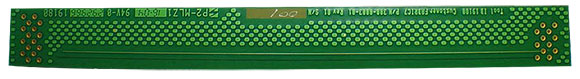
The ‘traditional’ method of providing test structures is to create a special test coupon on which the test structures are located. This coupon is not a part of the PCB itself, but is built in the material surrounding the PCB on the fabrication panel. The advantage of this is that there is a coupon which can be taken to the laboratory and analysed without the need to cut samples from any of the PCBs in a lot. These coupons can be standardised, allowing fixtures to be built that speed up testing. This is good for the PCB fabricators. Figure 1 is a typical test coupon containing only impedance test traces.
The disadvantages of a dedicated test coupon are:
1. There is no way to guarantee that the trace widths in the test coupon are the same width as those in each layer of the PCB it is intended to represent. (I have had cases where the test coupon measured one set of impedances while the impedances on the PCB were entirely different. The reason was a CAD error on the part of the fabricator when the coupon artwork was created.)
2. The test coupon is separated from the PCB at final fabrication and is often not available when it is needed. (I usually get called in to troubleshoot the PCB after it has been assembled and the coupon is stored somewhere in the assembly process.)
The above disadvantages of dedicated test coupons far outweigh their advantages so it is best to include the test structures in the body of the PCB itself. This has several obvious advantages. Among these are that the test structures are always with the PCB they are intended to represent and the features in the test structures are created by the PCB designer rather than PCB fabricator.
Examples of test structures
Impedance test structures
Figure 2 is a diagram of one way to design impedance test traces. This diagram shows both a single-ended impedance test structure and a differential test structure. If a PCB has eight signal layers on which impedance is being controlled, the structure can be expanded to provide a test structure for each layer.
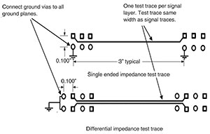
The spacing and size of the vias at the ends of the test traces are important. In order to permit the use of standard impedance test probes, the distance between the via at the end of the trace and its ground via needs to be 100 mils. The diameter of the drilled hole needs to be 30 mils to allow the probes to fit properly.
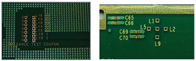
Figure 2 shows traces three inches long that are straight and have access vias at both ends. The length needs to be at least three inches in order to provide accurate impedance measurement. It is not necessary to have access vias at both ends of a test trace, although it is handy. It is also not necessary for the traces to be straight. If there is not room on a signal layer for a straight trace, it can be bent. Figure 3 depicts photos of two ways to implement impedance test traces on a PCB.
The example on the left hand side of Figure 3 has a ground via for each test trace. The example on the right hand side of Figure 3 has a single ground via in the centre with four test traces sharing it. Both are acceptable ways to implement impedance test traces. It is important to maintain the 100 mil hole spacing and 30 mil drill diameter in order to facilitate testing. Notice that each test trace is labelled in the silk screen with its layer number. This is an important feature when it comes time to do the actual testing.
Power plane capacitance measurements
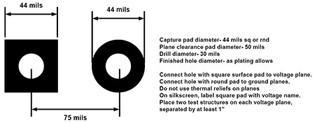
Figure 4 illustrates how to design access points that are used to measure the impedance of the power planes and the bypass capacitors. This is an important test that verifies the decoupling capacitor population is correct for each power supply voltage.
Two of these test access points are required for each power supply voltage on a PCB. One point allows a signal to be injected into the plane capacitor and the second allows measurement of the resulting voltage. The two structures should be placed at least one inch apart and labelled with the voltage to which they connect.
Stacking stripes
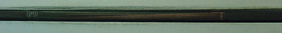
Figure 5 illustrates a test structure that is used to check several things about the way a PCB is built. It is called a set of stacking stripes. Strips of copper are plotted along one edge of a PCB in such a way that when the PCB is cut from the panel the strips are visible to the naked eye. Notice that the strip in each layer gets longer than the one above.
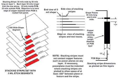
This stair step makes it possible to determine that all the layers are in the correct order by simply observing that the stair steps get longer with each layer down into the PCB. One might wonder why they would ever be out of order. There are many places in the design and fabrication process where the order of the layers can be mixed up. One is in the preparation of the photo-tools used to etch the PCB layers and another is in the actual laying up of the individual layers as part of the lamination process.
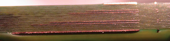
Figure 6 is a photograph of the stacking stripes in a 24-layer PCB showing just such a mix up. Layer 22 is where layer 11 should be and layer 11 is where layer 22 should be. How did this happen? When the Gerber data was being prepared, the CAD operator mislabelled the CAD files. The fabricator just followed that wrong order. If this PCB had been assembled, it would not have functioned properly. Without the stacking stripes, there would have been no way to determine what was wrong.
A second feature in the stacking stripe set is a small section of trace plotted such that when the PCB is cut from the panel it is visible end on. This trace is plotted 5 mils wide. By measuring the actual etched width it is possible to determine if the signal layer is properly etched and not over or under etched. Using this and the stackup dimensions, it is possible to troubleshoot what is amiss when the impedance is not within specifications and determine what corrective action needs to be taken.
Lastly, it is possible to examine the overall cross section of the PCB by measuring the thickness of the dielectric layers and the copper layers. This provides a complete audit of the stackup without the need for destructive testing. Best of all, these features are a part of every PCB, so it is easy to check the cross section and impedance long after the PCB has been assembled, should this be necessary. Figure 7 is an enlarged view of an actual set of stacking stripes showing the actual glass fibres in each dielectric layer, the copper thickness and the 5 mil traces protruding from the PCB.
One objection that is raised when stacking stripes are proposed is the old standard that ‘no exposed copper be allowed at the edges of a PCB.’ The way that standard actually reads is that no copper attached to any circuit inside the PCB is allowed to be exposed at the edge of a PCB. This requirement is easily met by making sure these copper strips are isolated from all of the circuits inside the PCB itself.
Cost of test structures
Adding the test structures described above adds little or no cost to the finished PCB. The only real cost is the time the PCB designer must invest to add these features to each new PCB file. In my experience, CAD departments are slow to get the first structures designed, but once they get some experience, this task adds very little to design time.
Cost of not having test structures
From all of the discussions so far, the cost of not having test structures should be clear. However, in many cases the cost is not obvious. Without test structures there is no way to isolate PCB failures to an incorrect impedance or a wrong stackup, the wrong glass fibre or the wrong copper thickness. The undetected mistakes are grouped under that broad, frustrating group of ‘flaky’ PCBs. As a result, there is no mechanism for taking corrective actions.
If no stacking stripes were used on the PCB in Figure 6, manufacturing would have assembled about $5000 worth of parts on the PCB. It would never have worked properly. Those people responsible for debug would have invested countless hours with no positive results. What is that worth? Perhaps the whole programme would be put at risk. Some ‘no-cost’ stacking stripes prevent this.
Examples of failures caught by test structures
The PCB in Figure 6 is one of the best examples of failures caught by using test structures. (In this case, all of the impedances were correct because the layers that were swapped were power and ground planes.) A not so obvious failure that I caught using the test structures was an assembly with the wrong type of bypass capacitors called out on the bill of materials. Incorrect impedance values are the remaining thing test structures catch.
Disadvantages of having test structures
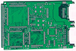
Other than the surprise exhibited by fabricators and others who are not accustomed to seeing these test structures, there are no disadvantages to adding them to a PCB design. Sometimes it is claimed that there is no room for them on a crowded PCB. In my experience, there has always been room. The designer might need to use a little imagination, but there is always room. Figure 8 is a picture of a PCMCIA card with stacking stripes along the top edge.
Summary
For engineers to design test structures into PCBs and fabricators to build them requires only a very minimal amount of time and cost. However, the long term savings can be significant and can mean the difference between overall product success and failure.
For more information contact EDA Technologies, +27 (0)12 665 0375, [email protected], www.edatech.co.za
| Tel: | +27 12 665 0375 |
| Email: | [email protected] |
| www: | www.edatech.co.za |
| Articles: | More information and articles about EDA Technologies |


© Technews Publishing (Pty) Ltd | All Rights Reserved
 printer friendly version