
I was astounded a while ago when an electronics company executive thought that a printed circuit board (PCB) was printed instantaneously through a printer connected to a PC. How far from the truth that assumption was.
Truth be told, it takes over 150 steps or processes to produce a PCB from receipt of the design data in CAM format. With modern electronics requiring highly sophisticated boards, lack of careful control in any of these manufacturing steps may result in a non-conforming product or even worse – a marginally conforming one.
Attaining the highest possible quality can only be achieved by focusing on all the individual details, from design input through process improvements and onto delivery. It is vital to identify the processes across the entire flow in detail, and it’s only when you have that level of overview that you can plan for quality throughout the supply chain.
A far cry from the first PCB patent in 1903, modern electronic products are expected to offer more and more advanced functions, while the products themselves are becoming smaller and smaller. This puts greater demands on the PCB design and also the aspects relating to the board manufacturing process.
There are two key factors for the successful production of high-quality advanced PCBs: firstly, making the right choices at the design stage; and secondly, carefully choosing the factory that can support the specific technical demands of the project in question.
Get the design right from the start
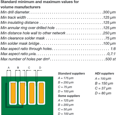
One aspect that needs to be prioritised with advanced boards is the design itself. The margins are tiny with regard to such factors as conductor widths, isolation distances between copper features, impedence requirements, hole sizes and their relation to capture and target lands. All this poses a considerable challenge at the layout stage.
The design rules should be realistic and adapted to volume production right from the start. One contrary example may be making the inner layer cores too thin to produce good capacitive coupling. This might work in a prototype factory, where great care is taken to basically hand-process these thin inner layer cores, but it could lead to major problems when the product is in volume production, since they may have different capabilities and in this instance the thinner cores may easily get stuck during the processing through long, volume oriented etching lines since they are basically too flimsy.
According to Kenneth Jonsson from the NCAB Group, “If you focus on the wrong things from the start, it could jeopardise the entire project if you find that your design can’t be applied in volume production.” Hence, the most important factor behind achieving an optimal design is to make sure you work together with all the parties involved, i.e. the OEM companies, CAD designers, EMS companies and PCB manufacturers.
Choice of materials
The fact that there are hundreds of PCB materials and laminates to choose from does not necessarily mean that a PCB manufacturer has it in stock. Different materials naturally influence price in different ways; some special materials that are used for high-frequency applications can cost from 5 to 30 times as much as standard FR4.

Carefully planned designs and clearly expressed PCB specifications enable PCBs with clock frequencies of up to 10 GHz to be designed on standard FR4 laminates. For example, it is much better to state an impedance requirement than to state a certain make of FR4 and then hope that the PCB that is supplied will work. Limiting your design to a particular brand imposes strict limits on the manufacturer as regards both UL certification and the materials in stock.
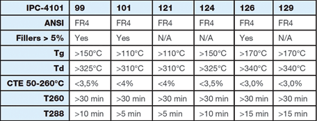
Now that we are working in accordance with the RmHS directive with lead-free production, values such as Tg (glass transition temperature), Td (decomposition temperature) and CTE (coefficient of thermal expansion) are more frequently found in customer specifications.
In cases where these values are not reasonably specified, the manufacturer is forced to choose an unnecessarily expensive material – sometimes twice as expensive as a standard material. It is therefore preferable if the specification refers to the new classes in IPC-4101B, as laminate manufacturers have now begun to use these to classify their laminates.

Selecting the right PCB manufacturer
Not a week goes by without my inbox being flooded with offers for the best quality PCBs, almost all of them from ‘the best’ Chinese manufacturers. But as any experienced manufacturer will tell you, not all PCBs live up to the same quality standards and failure rates across different bareboard manufacturers can vary to a large degree.
Quality is critical, and small mistakes can affect not only costs, but the success or failure of an entire product or project. What may appear to look good from the outside may conceal numerous flaws and reliability issues that could be disastrous during the assembly and expected lifetime of electronic products.
BPA Consulting has been producing a five-year forecast of global PCB production and markets since 1978. According to BPA, “global PCB market value will increase to $68,5 billion in 2016 meaning China’s share of PCB production will increase further to 51%.” In the context of this inevitable domination of the global market by China, it becomes imperative that customers wisely choose PCB manufacturers that have a reputation for consistent quality and with a proven track record.
We know for sure that anything can happen during a complex production process. And it often does. The important thing is to understand the problem and find a solution, then to implement future preventative and corrective actions. Key performance indicators such as quality and delivery performance should form part of the selection criteria.
As printed circuit board technology continues to evolve (now the most complex bespoke component in a PCB assembly), manufacturing consistently reliable PCBs is of paramount importance. What may appear to look good from the outside may conceal numerous flaws and reliability issues that could be disastrous during the assembly and expected lifetime of electronic products.
As NCAB Group’s Chris Nuttall puts it, ”If a factory says it has laser drills and is thus capable of producing high-tech PCBs, it’s rather like saying that all you need to do to become a new Michelangelo is to get yourself a hammer and chisel. It’s just as important to know how to handle the plating process as to have cutting-edge plating equipment.”
It is vital that designers and buyers choose the right partner on this journey, a partner with the technical experience and grasp of both prototype and volume production. This is the only way to avoid the pitfall of designing a board that works well at the prototype phase, but not when it comes to volume production. It is also important to have several factories that are well established in the industry, so that the PCB manufacturer can always deliver the optimal solution, irrespective of the volumes involved.
However, the most important factor behind achieving an optimal design is making sure you work together with all the parties involved, i.e. the OEM companies, CAD designers, EMS companies and PCB manufacturers.
All too often, when we receive an enquiry from our EMS customers, we find ourselves presented with a finished design and no time to make any improvements. There is a lot of time and money to be saved by implementing the right approach – most importantly you’ll get a product that will last for decades!
| Tel: | +27 12 665 0375 |
| Email: | sales@edatech.co.za |
| www: | www.edatech.co.za |
| Articles: | More information and articles about EDA Technologies |

© Technews Publishing (Pty) Ltd | All Rights Reserved