


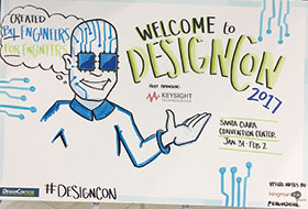
Silicon Valley. The location for the world’s largest expo for ‘Where the chip meets the board’: Designcon 2017 was sure to be a melting pot of the PCB industry shapers, and that it was.
I was honoured to be nominated to the Technical Program Committee (TPC) of DesignCon USA, and am pretty sure there wasn't anyone else representing a company or institution from the southern hemisphere. There wasn't a chance I was going to miss this opportunity to rub shoulders with some of the industry's experts and to bring some of that knowledge back to South Africa’s soil for the benefit of Cirtech EDA’s enormous pool of customers and engineers.
One of the tasks of a TPC member is reviewing technical papers submitted by speakers and other contributors. Just seeing some of the subjects like ;Design and verification for 112 Gbps; really turned my head and signal integrity inside out. While some engineers today sadly merely define a PCB as FR4 (whatever that may be), some subjects under review were really probing deep into available options for ultra low-loss materials for the higher speeds we will soon unquestionably be facing.
So I made the trek to California, and after a 34 hour journey via Hong Kong, it sure felt like the Great Trek. I was destined for Santa Clara, the heart of Silicon Valley. The last time I visited the valley was precisely 20 years ago to attend an instructor’s course on the world's best autorouter at the time, Specctra from Cooper & Chyan. That was a trip well worth it, and one that my fellow SA engineers and PCB specialists would benefit from for over a decade.
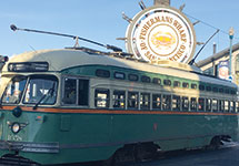
But what would a journey for such a long duration be without the chance to unwind the jet lag by doing some sightseeing? Precisely, and I had a day or two to do so. I've learned during my travels over the years that one of the best ways to explore a new city in the shortest time is by getting a 24-hour hop-on hop-off bus ticket. That did the trick in San Francisco. If you ever head to DesignCon in the future, make sure you spend some time in this colourful city which includes attractions like The Dungeon, Madame Tussauds, Ripley’s Believe it or Not, and Pier 39. Pier 39 seems to pride itself on the best crabs and clam chowder, and I must say the servings are huge!
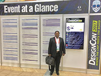
With the jet lag sort of sorting itself out in my brain, I headed off for the first day of DesignCon 2017. With a kaleidoscope of classes to attend, it was really a challenge to decide which topic won the vote. For day one I knew it had to be the Boot Camp presented by the one and only Lee Ritchey. Author of two world recognised books on high-speed design, Lee is no newcomer to the subject.
It always astounds me that at his advanced age, Lee is so generous in sharing the hands-on experience he has accumulated over the last 50 plus years. Over dinner one evening with Lee and his business partner John Zasio (also acclaimed in so many ways, and co-author of Lee’s books), Lee explained that much of his proven advice comes from experiments done for the Apollo programme in the sixties. With an unlimited state budget and the freedom to experiment until a theory was proven or disproven, Lee could go to town until he exhausted a subject such as ‘At what frequencies do 45-degree corner traces become an issue’.
That’s what I really like about Lee’s classes, the data he presents is proven. On his business card after his name I noticed the letters ‘SHK.’ I'll save you the agony, it's not one of his degrees, rather it stands for ‘School of Hard Knocks’. Be sure to attend Lee’s classes in SA during October this year, hosted by none other than EDA Technologies who brought Lee to SA in 2016 for the first time.
In Lee’s boot camp session, much emphasis was placed on carefully selecting PCB materials. Aspects like weave type, direction and density are becoming key factors in reducing signal losses and preventing skew. Ignore this at your own peril. What was previously a green object with some copper and holes produced through chemical and mechanical processes, the PCB now also includes a third process, the scientific aspects of design for function.
A high-speed trace with very fast switching needs to be handled with extra care, and here it is becoming critical to partner with a reliable and consistent PCB supplier who understands in detail the challenges of getting the circuit to function on a PCB. If your current PCB supplier is just a quote generating machine with little or no hands-on ability to support you with advice on topics such as insertion loss, skew differential, ultra low loss material selection, mechanical weave spread, via impedance, backdrilling, etc., then you should be concerned. High-speed switching and super-fast signals are coming our way whether we like it or not, at least that was clearly demonstrated by the PCB experts and chip manufacturers at DesignCon.
I must admit, some of the material presented over the three days by other speakers was way over my head. I kept wondering how many people in the 100+ class could follow all the detailed formulae and hold attention for an hour or so. And is it necessary? Probably so, but it was great to see the end of the session where the speaker summarised his findings and offered a simple answer to an important question such as ‘Can flexible circuits carry DDR4 signals’? A simple yes or no would have worked for me, but at least I know someone has taken the effort to make his point valid. And best is that I don't have to prove it all over again.
In case you didn't know, all PCB materials have datasheets much like the components that go on to the PCB. If you never bothered to get the laminate datasheet before, best you get into that habit immediately. With the copper laminate shortage in China, don't be surprised if your current PCB factory substitutes the laminate with cheaper yet more available derivatives. For repeatability and a reliable PCB product, it is best that you specify the exact laminate in your instructions to your PCB supplier.
At DesignCon, all serious laminates producers had the chance to show off their latest materials in the Expo hall. Much focus was on low loss materials, and producers such as Rogers, Park Nelco, Taconic, ITEQ, Shengyi and Doosan all had super performing laminates to choose from. Of course choosing materials is just part of the solution, to have a successful PCB product you need a partner that can also offer practical advice on availability of materials and advise on the most cost-effective choices. Cirtech EDA’s premier PCB supplier, NCAB Group, stocks a good variety of these special materials to support your design needs. And locally, Cirtech EDA’s technical support staff are adequately ready to support your growing needs.
At DesignCon, a few keynote speeches covered hot topics such as connected cars and IoT. I witnessed some of Google's autonomous cars doing their rounds close to Google’s facilities, and during DesignCon I heard that one car was involved in an accident! This is work in progress but not as far-fetched as some would imagine. I managed to chat briefly to the head of Microsoft’s cloud services. Anyone who would like his contact details in order to discuss partnerships for locally adapted autonomous vehicles, feel free to contact me.
Needless to say, a PCB is not just a PCB anymore. While the PCB’s current epoxy glass structure is here to stay for a while, the materials and construction methods are evolving fast to support today’s high speed and high temperature demands. The two most important aspects that will test a PCB product are good signal integrity (SI) and efficient power distribution network (PDN) design. These design aspects should be considered long before the first component is even placed using an EDA CAD system.
The demands of SI and PDN must define the PCB layer stackup rather than any routing real estate demands. Having said this, layer counts are increasing worldwide with 6-layer PCBs becoming the new 4-layer. It is not uncommon to see 16-layer boards ordered, designed to include multiple buried capacitance cores for high-speed designs with no EMC issues from the first revision. The power of knowing!
My first involvement with DesignCon was four years ago as a speaker at DesignCon China for NCAB Group on the topic ‘Design for Manufacturability’, but this time I could just attend the classes and absorb. That I did. As local leaders in high-tech and high-end PCBs, Cirtech EDA is even more ready now to serve the local PCB industry, as it has over the past 20 years. This DesignCon involvement was indeed a firm investment in the future of PCBs for SA, and a clear message to our local designers that we are ready to support SA companies to make world-class products.
I bid my farewell to an expertly executed DesignCon 2017 and prepared my mind for the long trek back home. It helped not to travel economy class, and the Häagen-Dazs ice cream served by Cathay Pacific was delicious. Touchdown was at OR Tambo international airport, minus the mayhem caused by Mr Trump at US airports. How thankful I am to be able to support the highest PCB technologies needed by our world class engineers, but have the luxury of the African bush within a two hour drive. Don’t you just love South Africa?
For more information contact Nechan Naicker, Cirtech EDA, +27 (0)12 665 0375, nechan@cirtech-eda.com, www.cirtech-eda.com
| Tel: | +27 21 700 4900 |
| Email: | info@cirtech-electronics.com |
| www: | www.cirtech-electronics.com |
| Articles: | More information and articles about Cirtech Electronics |


© Technews Publishing (Pty) Ltd | All Rights Reserved
 printer friendly version