All that glitters is not gold’ is a well-known expression which in various forms originated in or before the 12th century. In act II, scene VII of The Merchant of Venice, William Shakespeare wrote:
“All that glisters is not gold;
Often have you heard that told:
Many a man his life hath sold
But my outside to behold:
Gilded tombs do worms enfold.
Had you been as wise as bold,
Young in limbs, in judgement old
Your answer had not been inscroll’d
Fare you well, your suit is cold.”
As printed circuit board (PCB) technology continues to evolve – now the most complex bespoke component in any PCB assembly – manufacturing PCBs that are reliable has paramount importance. What may appear to look good and shiny from the outside may conceal numerous flaws and reliability issues that could be disastrous during the assembly and operation of this key component in all electronic products.
Well researched IPC standards (www.ipc.org) have been released to measure and assure the reliability of PCBs. However, in some cases, vital steps in high-reliability PCB design, fabrication and assembly are overlooked for a variety of reasons – inadvertently, to save time or to get the project out the door, or just to save money. The results are often costly, if not disastrous and life-threatening.
The reliability of bare PCBs is established by three variables: the quality of the conductive copper, the robustness of the laminates and materials used in the production process, and the actual PCB design. PCB reliability is a product of all three influences and how they interact with each other.
Only careful attention to material selection will result in a predictable product with consistent quality. Just specifying FR4 does not ensure any consistency between production batches, as bare board manufacturers may change their laminates according to price, availability and what is in stock in their stores. Since an FR4 PCB is constructed with woven cloth, the surface will never be absolutely smooth, with certain brands more uneven than others due to the weave spacing and resin material (see Figure 1).

In a high-reliability application, specifying the brand of laminate may be crucial as it ensures consistency of the dielectric constant and PCB thermal expansion properties. Since hundreds of laminates manufacturers are found around the world, using reputable ‘brand-name’ laminates is an important criterion in any PCB production, and guarantees a product that is stable under the intended environmental conditions and reliable over time. Some well-known brands include Rogers, Nelco, Isola, Shengyi, Iteq and Taconic, amongst others.
Copper quality can be evaluated quite accurately by micro-sectioning methods to determine the general quality of the board. Reputable laminate manufacturers also provide datasheets of their product and this allows the designer to select the most appropriate material for their application.
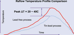
Next in the hierarchy of PCB reliability is the robustness of material. With the advent of RoHS, materials tend to be as much a problem as copper quality in the robustness of PCBs. Assembly of lead-free PCBs is often performed at temperatures 30°C higher than the previous tin-lead process (see Figure 2). At the new lead-free assembly temperatures, the materials used in the PCB construction tend to break down, adding to the failure modes caused by lead-free assembly in general.

Essentially then, the assembly of lead-free products requires the use of PCB materials that will not break down at higher processing temperatures. To better facilitate the industry transition to lead-free PCBs, reputable manufacturers offer a broad assortment of appropriate substrates.
The glass transition temperature (Tg) is an important aspect of material selection, as it determines the temperature which the resin material in the PCB construction can endure for only a very short time before it converts from a glassy, brittle condition into a soft elastic one which may be dimensionally unstable.
The Tg value of the base material sets here an upper limit at which the resin actually decomposes and subsequent delamination occurs. For PCBs subject to soldering processes using the more elevated soldering temperatures required for lead-free solders, specifying a Tg of 140°C will not be adequate for PCBs thicker than about 1,30 mm.
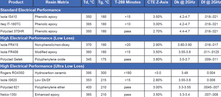
When the Tg is over 170°C, it is referred to as a high Tg material. Generally, the differences between common FR-4 material and high Tg FR-4 material is that high Tg materials have better mechanical strength, dimensional stability, adhesiveness of the laminates, as well as lower moisture absorption, thermal decomposition and thermal expansion than that of common PCB base materials (see Figure 3). Many global manufacturers of high-reliability products that involve lead-free processes insist on high Tg materials as a standard requirement. And it makes sense.

It is vital that PCBs function reliably both during the manufacturing assembly process and out in the field. Apart from the costs involved, faults during assembly can end up being built into the final product via the PCBs, with possible failure in the field resulting in serious compensation claims. In all market sectors, particularly those producing products with critical applications, the consequences of such failures could be devastating. Relative to that, in the author’s opinion, the cost of a premium quality PCB is actually negligible.
Another key factor in PCB reliability is the coefficient of thermal expansion (CTE). It describes the percentage points that a PCB expands as it is heated or cooled. Every known material in the world expands or contracts with a change in temperature; the same is thus true with PCBs. The major cause of thermal cycling reliability degradation is due to the z-axis expansion of the dielectric material.
The expansion of the dielectric is constrained to some extent in the x and y axes due to the warp and weft of the fibre glass. However, there is no constraint in the z-axis. Figure 4 is a cross section showing the z-axis expansion that would be typical when the circuit board is heated to 260°C. The z-axis expansion of the dielectric is usually two orders of magnitude higher than the copper expansion.

It becomes obvious then that the z-axis expansion is the major contributor to breaks in the copper interconnections in the PCB. Such failures are not discovered during the netlist testing of the finished bare PCB, but become evident either during thermal cycling or, worse yet, due to failure in the field.
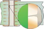
It makes sense that when the copper interconnections such as vias are stronger than the forces that act upon it, the wall plating will not break and therefore be considered reliable. A thinner wall will reveal a weak area (see Figure 5) that will be more prone to failure during the periods that the PCB undergoes higher temperature conditions, and specifically during the higher temperature cycles necessary for lead-free assembly.

Lead-free solder also tends to dissolve copper. The copper dissolution may be serious enough to violate copper thickness requirements, resulting in thinner walls that fall outside the 18-20 μm requirements for IPC Class 2 PCBs.
To ensure reliable interconnections, reputable PCB manufacturers such as the NCAB Group (www.ncabgroup.com) specify an IPC Class 3 plating of approximately 25 μm as a standard production specification across each and every PCB manufactured, thus ensuring a much stronger resistance to the forces of expansion that act upon it.
IPC Class 2 (standard for most factories) provides 20% less copper and will be more prone to metal fatigue. Other risks of not having sufficient wall plating thickness include blow-holes or outgassing, electrical continuity problems (inner layer separation, barrel cracking) during assembly or risk of field failures under load conditions.
Not all manufacturers plate the same thickness, so for consistency from manufacturer to manufacturer, the plating thickness should be clearly noted in the instructions to the manufacturer. Bad reliability may occur when those involved in the supply chain have little or no interest in the product, when random decisions are made without being based on fact, when specifications are unclear, or when the focus is on price instead of total cost.
NCAB Group provides a 31-page manufacturing specification which includes a high quality standard for reliable PCBs. Some of the quality specifications applied to all its PCBs include: 25 μm wall plating thickness; no track welding or open circuit repair allowed; cleanliness requirements beyond those of IPC; only internationally known base material types used; specific requirements for depth of via fill; tight control on age of specific finishes; specific solder mask thickness; and no x-outs accepted on panels.
| Tel: | +27 12 665 0375 |
| Email: | [email protected] |
| www: | www.edatech.co.za |
| Articles: | More information and articles about EDA Technologies |
© Technews Publishing (Pty) Ltd | All Rights Reserved