


As the speed and resolution of data converters continue to increase, the need for higher-frequency sampling clock sources with lower phase noise is growing. The integrated phase noise (jitter) presented to the clock inputs is one of the many performance bottlenecks facing designers when they create cellular base stations, military radar systems, and other designs that require high-speed, high-performance clock signals.
An average system has several low-frequency, noisy signals that a phase-locked loop (PLL) can up-convert to a higher frequency to clock these devices. A single high-frequency PLL can solve the frequency translation problem, but it is difficult to create one with a loop bandwidth that is low enough to filter out the effects of the noisy reference. A PLL with a low-frequency, high-performance VCO/VCXO and low loop bandwidth can clean the noisy reference, but cannot provide the high-frequency outputs.
Both high speed and noise filtering can be obtained by combining two PLLs: a low-frequency device with narrow loop bandwidth for jitter cleaning, followed by a high-frequency device with a wider loop bandwidth.
Some modern dual-loop analog PLLs are integrated on a single chip, allowing designers to reduce low-frequency reference jitter while providing high-frequency, low-phase-noise outputs. This saves valuable PCB area and allows multiple devices that require different frequencies to be clocked from a single phase-aligned source.
The AD9523, AD9523-1 and AD9524 clock generators from Analog Devices, shown in Figure 1, consist of two series-connected analog PLLs. The first PLL (PLL1) cleans the reference jitter, while the second PLL (PLL2) generates high-frequency, phase-aligned outputs. PLL2 can also generate a high base frequency from which various lower frequencies can be derived.
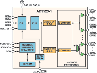
PLL1 uses an external low-frequency VCXO and a partially embedded third-order loop filter to create a PLL with a loop bandwidth in the 30 Hz to 100 Hz range. The bandwidth of this loop directly affects the amount of reference input phase noise that will propagate to the output.
PLL2 uses an internal high-speed VCO centred at 3,8 GHz (3 GHz for the AD9523-1) and a partially embedded third-order loop filter to give it a nominal loop bandwidth of about 500 kHz. The bandwidth and phase noise of this internal VCO directly affect the wideband phase noise of the overall output.
Many engineers think of dual-loop PLLs as frequency translators that reduce the reference input jitter by a fixed amount, but it is more accurate to think of them as low-phase-noise frequency translators whose performance is affected by each PLL’s loop bandwidth and the phase noise profiles of the VCO/VCXOs.
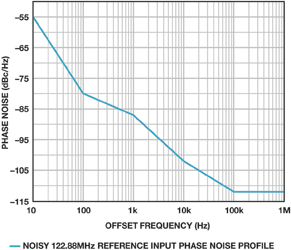
The ADIsimCLK simulation tool provides an easy way to determine the effects of reference phase noise on the output phase noise of a dual-loop PLL. This example uses ADIsimCLK to model the effects of a noisy reference on the overall phase noise of the AD9523-1. Figure 2 shows a simulated 122,88 MHz reference with a typical phase noise profile.
PLL1 relies on a high-performance VCXO and low loop bandwidth to attenuate the phase noise of the reference, allowing the phase noise of the VCXO to dominate. This example uses a Crystek CVHD-950 VCXO to generate an output frequency that is identical to the reference input. This shows a direct comparison of how much reference phase noise appears on the output of PLL1. Figure 3 compares the phase noise profile of the Crystek CVHD-950 VCXO and the reference input phase noise.
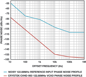
Figure 4 and Table 1 show the ADIsimCLK configuration parameters used to simulate the AD9523-1’s PLL1 output phase noise response for the reference input and PLL1 VCXO phase noise profiles shown in Figure 3. Table 2 shows the PLL1 loop filter values generated by ADIsimCLK given these settings.
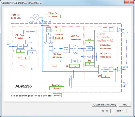
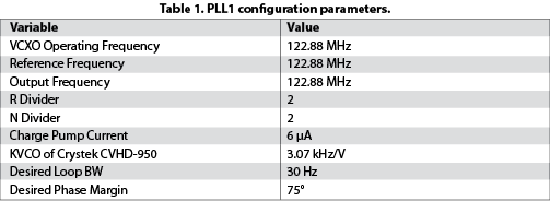
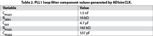
Figure 5 shows the simulated output of PLL1 at 122,88 MHz (solid line) from ADIsimCLK along with the original phase noise profile of the noisy 122,88 MHz reference (dashed line).
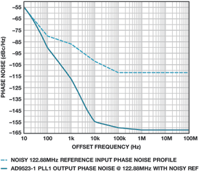
Note that the phase noise of PLL1’s output is much lower than the original reference input phase noise. The loop bandwidth of PLL1 attenuates the phase noise of the reference significantly, allowing the low phase noise profile of the VCXO to dominate after the 30 Hz loop filter cutoff frequency. If the reference phase noise is increased across all offset frequencies, the output phase noise will only increase as a function of PLL1’s loop bandwidth.
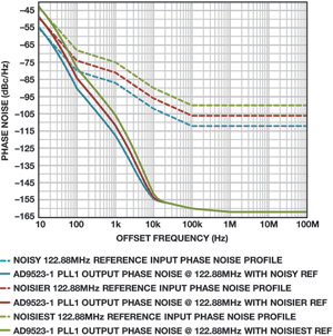
Figures 6 and Figure 7 show the AD9523-1 PLL1 output with 6 dB and 12 dB higher phase noise than the noisy reference shown in Figure 2. Beyond an offset frequency of about 20 kHz, PLL1’s output phase noise is dominated by its loop settings and the VCXO’s performance. Thus, with an integration range starting from a 20 kHz offset, jitter performance will only change slightly, despite the 12 dB increase in reference input phase noise.
This is a direct result of designing PLL1 to have a low loop bandwidth and using a low-phase-noise VCXO. A low-frequency, high-performance VCXO with a low KVCO must be used to create a PLL1 loop bandwidth small enough to perform this jitter cleaning. The low-phase-noise output of PLL1 now serves as the reference to PLL2 to create a phase-aligned, higher-frequency output.
PLL2 contains an internal VCO centred at 3 GHz to allow output frequencies of up to 1 GHz. To compare the noisy input reference with the overall phase noise of the AD9523 family, examine the resultant phase noise at 122,88 MHz (FVCO divided by 24). Note that PLL2’s outputs are normally used for frequency translations or high-frequency outputs.
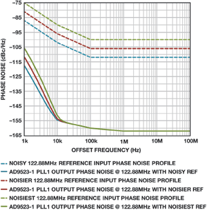
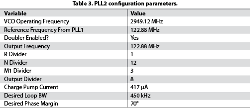
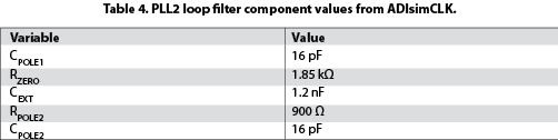
Table 3 shows the PLL2 configuration parameters entered into ADIsimCLK, and Table 4 shows the PLL2 loop filter values generated by ADIsimCLK, given these settings.
Figures 8 and Figure 9 compare each reference input phase noise with the resultant output phase noise from the AD9523-1 as simulated with ADIsimCLK. Notice the added phase noise pedestal between 10 kHz and 1 MHz; this is due to the internal VCO phase noise of PLL2.
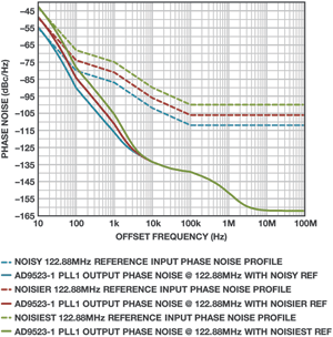
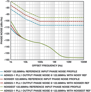
The internal VCO phase noise in PLL2 is high enough after about 5 kHz offset frequency that it begins to dominate the overall output phase noise of the device. The added reference phase noise has minimal effect on output phase noise after the 5 kHz offset region.
Conclusion
The jitter cleaning aspect of PLL1 prevents most of the reference input phase noise from reaching PLL2. A noisy reference input does affect close-in phase noise (sub 10 kHz offset), but the overall output jitter of the device is dominated by the performance of the device, rather than the performance of the reference. In cases where integrated jitter is calculated from 12 kHz to 20 MHz, output jitter will likely be the same regardless of input jitter.
Rather than claiming how much jitter a dual-loop analog PLL can attenuate, the real performance measure should be how much jitter it generates.
For more information contactErich Nast, Avnet Kopp, +27 (0)11 319 8600, erich.nast@avnet.eu, www.avnet.co.za


© Technews Publishing (Pty) Ltd | All Rights Reserved
 printer friendly version