


Sensors, which are ubiquitous, are used to measure temperature, light, sound and a variety of other environmental parameters. Some sensors act as parameter-dependent voltage or current sources. Thermocouples, for example, generate a voltage that is proportional to the temperature difference between a reference junction and the measurement point.
Most sensors have transfer functions that follow a known relationship with respect to the physical parameter. The transfer function is often an impedance, where current is the sensor input and the voltage across the sensor indicates the parameter of interest. Resistive sensors such as load cells, RTDs and potentiometers are used to measure strain, temperature and angle, respectively. To first order, resistive sensors are frequency independent and have no phase response.
Many sensors require AC excitation signals as their transfer functions change in frequency and phase. Examples include inductive proximity sensors and capacitive humidity sensors. Biometric impedance measurements can yield information about respiratory rate, pulse rate, hydration and many other physiological parameters. In these cases, the magnitude, phase, or both may be used to determine the value of the sensed parameter.
In some applications, transducers turn a sample under test into a sensor. Colorimeters, for example, use an LED to shine light through a liquid sample under test. The light absorption of the sample modulates the amount of light detected by a photodiode to reveal characteristics about the liquid under test.
Blood-oxygen levels can be determined by measuring the difference in light absorption of red and infrared light in vascular tissue. Ultrasonic transducers measure gas flow rates based on Doppler frequency shifts of the ultrasound as it travels through the gas. All of these systems can be implemented using synchronous demodulation.
Figure 1 shows a synchronous demodulation system for measuring a sensor’s output signal. An excitation signal, fx, acts as a carrier that the sensor modulates in amplitude, phase, or both as a function of the parameter being measured.
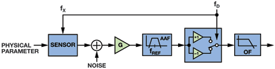
The signal may be amplified and filtered before being modulated back down to DC by the phase-sensitive detector (PSD). An output filter (OF) limits the bandwidth of the signal to the frequency range of the parameter being measured.
Noise at the sensor output may be due to internal sources or external coupling. Low-frequency (1/f) noise often limits performance of the sensor or measurement electronics. Many sensors are also susceptible to interference from low-frequency environmental noise. Optical measurements are susceptible to background light and electromagnetic sensors can be susceptible to radiation from the power supply. Freedom to choose the excitation frequency to avoid noise sources is a key benefit of synchronous demodulation.
Choosing an excitation frequency that reduces the effect of these noise sources is an important way to optimise system performance. The selected excitation frequency should have a low noise floor and be far enough away from noise sources so that modest output filtering can reduce the noise to acceptable levels. Sensor excitation is often the largest item in the power budget. If the sensor’s sensitivity vs. frequency is known, power consumption can be reduced by exciting the sensor at a frequency where its sensitivity is high.
The phase-sensitive detector
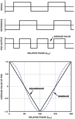
Understanding the requirements of the anti-aliasing filter (AAF) and OF requires an understanding of the PSD. Consider a PSD that uses the excitation signal to synchronously multiply the input signal by +1 and –1. This is equivalent to multiplying the input signal with a square wave of the same frequency. Figure 2a shows the time domain waveforms for the input signal, reference and PSD output for the case where the input signal is a square wave with arbitrary phase relative to the reference
When the input and reference are perfectly in phase, the relative phase is 0°, the switch output is DC, and the PSD output voltage is +1. As the relative phase increases, the switch output becomes a square wave at twice the reference frequency, and the duty cycle and average value diminish linearly.
At a relative phase of 90°, the duty cycle is 50% and the average value is 0. At a relative phase of 180°, the PSD output voltage is –1. Figure 2b shows the average output value of the PSD as the relative phase is swept from 0° to 360° for square-wave and sine-wave input signals.
The sine-wave case is less intuitive than the square-wave case, but it can be calculated by multiplying term by term and separating into sum and difference components as follows:
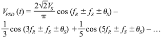
As desired, the PSD produces a response proportional to the cosine of the relative phase of an input signal at the fundamental frequency, but it also produces a response to every odd harmonic of the signal. With the output filter considered part of the phase-sensitive detector, the signal transmission path looks like a series of bandpass filters centred at the odd harmonics of the reference signal.
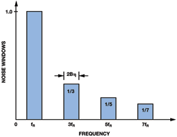
The bandwidth of the bandpass filters is determined by the bandwidth of the low-pass output filter. The PSD output response is the sum of these bandpass filters, as shown in Figure 3. The part of the response that appears at DC falls in the pass band of the output filter. The part of the response that appears at even harmonics of the reference frequency will be rejected by the output filter.
At first glance, an infinite sum of harmonics aliasing into the output filter pass band seems to doom this approach. However, the impact of the noise aliasing is mitigated because each of the harmonic terms is scaled by a decreasing factor, and the noise at the various harmonics adds as the root sum of squares. One can calculate the noise impact of the harmonic aliasing assuming the noise spectral density of the input signal is constant.
Let Vn be the integrated noise in the transmission window centred at the fundamental frequency. The total rms noise, VT is:
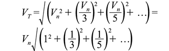
Using a handy formula for the sum of a geometric series that states:

the increase in the rms noise due to the harmonic windows is:
Thus, the rms noise due to all of the harmonic windows increases the total noise by only 11% or 1 dB. The output is still susceptible to disturbers in the pass band of the bandpass filters, and harmonic distortion from either the sensor or electronics before the PSD will cause errors in the output signal.
If these harmonic distortion terms are unacceptably large, they can be reduced with an anti-aliasing filter. The requirements for the anti-aliasing and output filters will be considered in the following design example.
LVDT design example
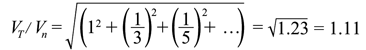
Figure 4 shows a synchronous demodulation circuit that extracts position information from a linear variable displacement transformer (LVDT), which is a specially wound transformer that has a moveable core that is affixed to the position to be measured. An excitation signal is applied to the primary, and the voltage on the secondary changes in proportion to the position of the core.
There are many types of LVDTs and ways of extracting position from them. This circuit uses the LVDT in 4-wire mode. The two LVDT secondary outputs are connected such that the voltages oppose each other, performing a subtraction.
When the LVDT core is in its null position, the voltages on the secondaries are equal, and the difference voltage across the windings is zero. As the core moves from the null position, the difference voltage across the secondary windings increases. The sign of the LVDT output voltage changes based on direction.
The LVDT chosen for this example measures a ±2,5 mm, full-scale core displacement. The voltage transfer function is 0,25, which means that the differential output will be 250 mV per volt applied to the primary when the core is displaced 2,5 mm from the centre.
Integrated synchronous demodulator
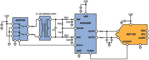
The ADA2200 integrated synchronous demodulator uses a unique charge-sharing technology to perform discrete time-signal processing in the analog domain. Its signal path consists of an input buffer, an FIR decimation filter that performs anti-aliasing filtering, a programmable IIR filter, a phase-sensitive detector and a differential output buffer. Its clock-generation functions synchronise the excitation signal to a system clock. Programmable features are configured through an SPI-compatible interface.
The 4,92 MHz clock generated by the AD7192 24-bit sigma-delta ADC is used as the master clock. The ADA2200 generates all of the internal signals it needs for clocking the filters and PSD, as well as generating the excitation signal on the RCLK pin. It divides the master clock by 1024 to generate a 4,8 kHz signal to control the CMOS switch.
The CMOS switch converts the low-noise 3,3 V source into a square-wave excitation signal to the LVDT. The 3,3 V supply used for the excitation source is also used as the ADC reference, so any drift in the voltage source will not degrade the measurement accuracy. At full-scale displacement, the LVDT will output a 1,6 V peak-to-peak output voltage.
Anti-alias filtering
The RC network between the LVDT output and the ADA2200 input provides low-pass filtering of the LVDT output signal and also produces the relative phase shift required to maximise the demodulator’s output signal. Recall from Figure 2b how the maximum PSD output occurs at relative phase shifts of 0° or 180°. The ADA2200 has a 90° phase control that enables ±90° relative phase offsets to be used as well.
Signal energy present at odd multiples of the demodulation frequency will appear in the pass band of the output filter. The FIR decimation filter implements anti-aliasing filtering, providing a minimum of 50 dB attenuation at these frequencies.
The IIR filter can provide additional filtering or gain if required. Since the IIR filter precedes the phase-sensitive detector, its phase response will affect the PSD signal output bandwidth. This must be taken into account in the design of the filter response.
Output filter
The pass band of the output filter should be selected to match the bandwidth of the parameter being measured, but limit the broadband noise of the system. The output low-pass filter must also reject output spurs that are created at the even multiples of the PSD.
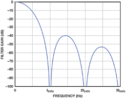
This circuit uses the LPF inherent in the AD7192 sigma-delta ADC. It can be programmed to have a sinc3 or sinc4 response, with transfer function zeroes at multiples of the output data rate. Figure 6 shows the sinc3 transfer function normalised to the ADC output data rate.
Setting the output data rate of the ADC equal to the demodulation frequency rejects the spurs at the PSD output. The ADC’s programmable output data rate acts as a selectable bandwidth output filter. The available output data rates (fDATA) are 4,8 kHz/n, where 1 ≤ n ≤ 1023. Thus, the ADC averages the demodulator output over n demodulation clock periods for each output data value.
Because the master clock and the ADC clock are synchronous, the transfer function zeroes of the ADC’s output filter will fall directly on every harmonic of the modulation frequency and all of the output spurs will be rejected for any value of n.
The programmable output data rate enables a straightforward trade-off between noise and bandwidth/settling time. The output filter has noise bandwidth of 0,3 X fDATA; 3 dB frequency of 0,272 × fDATA; and settling time of 3/fDATA.
The ADC digital filter has a 3 dB bandwidth of about 1,3 kHz at the highest output data rate of 4,8 kHz. The RC filter between the demodulator and the ADC is relatively flat up to that frequency to minimise the bandwidth required by the ADC. In systems with lower maximum data rates, the RC filter corner frequency can be reduced proportionally.
Noise performance
The output noise of the circuit is a function of the ADC output data rate. Table 1 shows the effective number of bits in the digitised data vs. the ADC sample rate assuming a 2,5 V full-scale output voltage. The noise performance is independent of the LVDT core position.
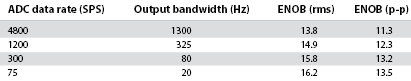
If the output noise from the ADA2200 were frequency independent, the expected effective number of bits would increase by one bit for every 4X decrease in the output data rate. The ENOB doesn’t increase as much at the lower output data rates due to the ADA2200 output driver’s 1/f noise, which begins to dominate the noise floor at the lower output data rates.
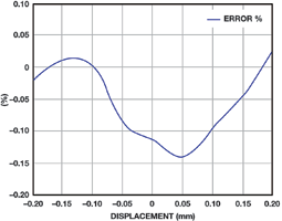
Linearity
The linearity was measured by first performing a two-point calibration at core displacements of ±2,0 mm. From these measurements, the slope and offset were determined to establish a best straight line fit. Next, measurements were taken at core displacements across the ±2,5 mm full-scale range. The measured data was subtracted from the straight line data to determine the linearity error.
The E Series LVDT used for the circuit evaluation specifies ±0,5% linearity over the ±2,5 mm displacement range. The circuit performance exceeds the LVDT specifications.
Power consumption
The circuit consumes a total of 10,2 mW, including 6,6 mW for driving the LVDT and 3,6 mW for the remainder of the circuit. The circuit SNR could be improved by increasing the LVDT excitation signal at the cost of increased power consumption. Alternatively, the power consumption can be reduced by lowering the LVDT excitation signal and using a low-power, dual op-amp to amplify the LVDT output signal to preserve the circuit’s SNR.
Conclusion
Many sensor signal conditioning challenges share characteristics that can be addressed with synchronous demodulation. Systems with excitation frequencies below 1 MHz and dynamic range requirements in the 80 dB to 100 dB range can be addressed with low-cost, low-power analog circuits requiring minimal digital post processing. Understanding the operation of the phase-sensitive detector and the likely noise characteristics at the output of the sensor are key to determining the system filter requirements.
For more information contact Stuart Hanford, Arrow Altech Distribution, +27 (0)11 923 9600, shanford@arrow.altech.co.za, www.arrow.altech.co.za
| Tel: | +27 11 923 9600 |
| Email: | info@arrow.altech.co.za |
| www: | www.altronarrow.com |
| Articles: | More information and articles about Altron Arrow |


© Technews Publishing (Pty) Ltd | All Rights Reserved
 printer friendly version