


The allocation of the 6 GHz band for wireless communication systems has opened new possibilities for high speed and low latency applications. Analog Devices’ 16 nm transceiver family offers a highly integrated solution for this new frequency band, featuring low power consumption and high performance.
With the forward momentum of wireless communication systems, new technologies and new spectrum are continuously being pursued and adopted. For those involved in the wireless industry, it is no surprise that the 3GPP’s inclusion of the 6 GHz frequency band in frequency range 1 (FR1) was welcome news. By expanding the original FR1, both lower and higher, from [450 MHz to 6000 MHz] to [410 MHz to 7125 MHz], the industry gains access to a significant amount of new spectrum, opening fresh opportunities for growth and innovation.
Compared to the legacy FR1 frequency band, the new 6 GHz band supports much wider bandwidths: n96 is 1200 MHz (5925 MHz to 7125 MHz), n102 is 500 MHz (5925 MHz to 6425 MHz), and n104 is 700 MHz (6425 MHz to 7125 MHz). Offering high-capacity spectrum with good network energy performance and better propagation than FR2 bands ensures that the new 6 GHz band will become an important resource for wireless connectivity.
ADI’s 16 nm transceiver family is available in both 8T8R and 4T4R configuration. This transceiver is a highly integrated device with extensive digital front-end functionality, including digital predistortion (DPD), crest factor reduction (CFR), and digital channel upconverters and downconverters (CDDC and CDUC). There are also energy saving features to be gained.
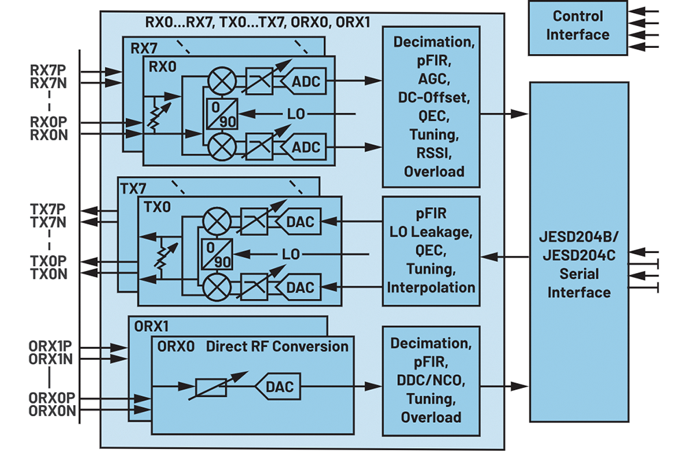 Figure 1. Block diagram of ADI 16 nm transceiver.
Architecture
As shown in Figure 1, ADI’s 16 nm transceiver series integrates eight differential transmitters (Tx0-7), eight differential receivers (Rx0-7), and two differential observation receivers (ORx0-1). The tunable frequency ranges from 400 MHz to 7125 MHz with two radio frequency (RF) synthesizers as the local oscillator (LO). The tunable bandwidth is as wide as 600 MHz. A high speed JESD204B/JESD204C interface is designed to connect to the baseband processor.
Transmitter
The transmitter applies zero-IF architecture. The in-phase and quadrature (I/Q) baseband signals from the DACs are reconstructed and filtered by the baseband low-pass filters (LPFs) and then upconverted by an analogue modulator and an LO to RF output. The zero-IF transmitter provides higher linearity and noise performance with relatively lower power consumption than the RF sampling converter.
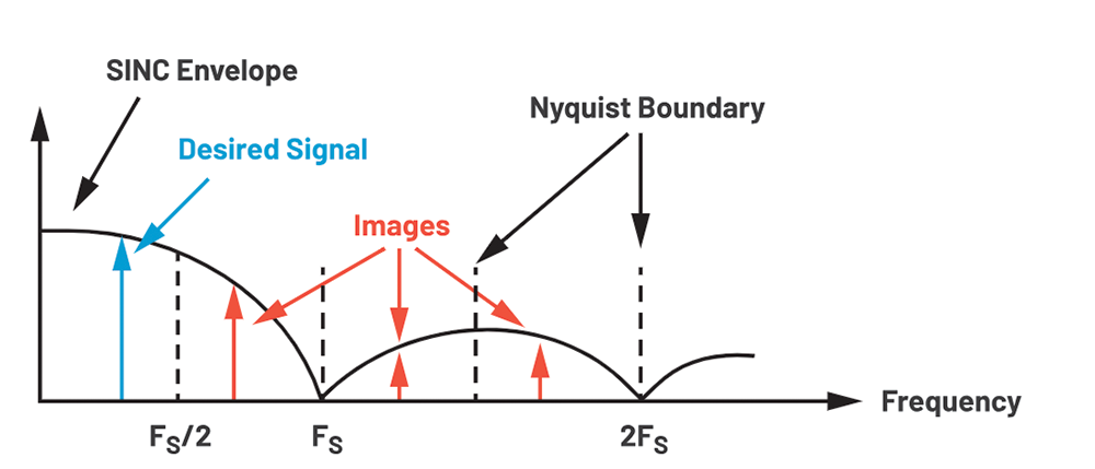 Figure 2. SINC response of DAC and its images.
The transfer function of the DAC takes a general form of sin(x)/x, and its frequency response is not flat as shown in Figure 2. The analogue output is attenuated at the higher frequency. Images of the desired signal are generated during the sampling process and need to be filtered out. Otherwise, they pollute the radio spectrum and violate the emission requirements from 3GPP and the FCC.
As a result, the maximum usable DAC output frequency is typically 40% of the sampling clock rate. For RF sampling to function effectively with 6 GHz band, the DAC sample clock must operate at above 18 GHz, which costs significant power. Here the advantage of the zero-IF transmitter is readily apparent. It only needs to digitise the baseband I/Q signal, and the DAC sample clock could be as low as 3 GHz to support the 6 GHz band. This provides flatter output power across the whole 6 GHz band (Figure 3) and lower noise spectral density (NSD) performance with relatively low energy consumption. Typically, even with the same process, RF sampling converters consume about 125% more energy than baseband I/Q converters for equivalent noise performance for a typical single band application.
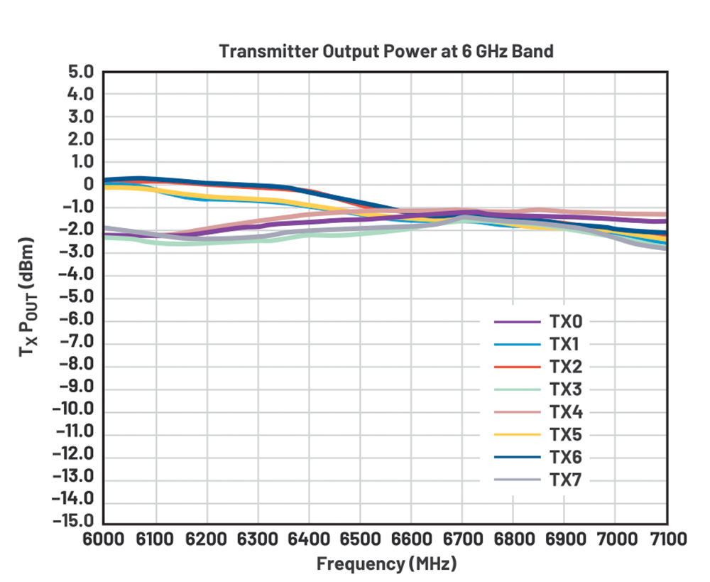 Figure 3. Transmitter output power and flatness at 6 GHz.
Receiver
On the receiver’s path, the RF input is downconverted to a baseband I/Q signal using an analogue demodulator and an LO. The continuous-time delta-sigma ADC is specifically designed to digitise the baseband I/Q signal. This ADC incorporates inherent antialiasing filtering, which significantly relaxes the filtering requirements compared to traditional sampling techniques. At the RF input port, the wideband matching provides a flat frequency response across the 6 GHz band as shown in Figure 4.
The baseband amplifier can be a classic topology using feedback circuitry for good linearity and noise performance. However, the RF sampling receiver needs expensive extra filtering at the RF frequency band. To sample the 6 GHz band, the RF sampling ADC requires an 8 Gsps sampling clock to convert the desired signal from the second Nyquist zone, making it impossible to avoid aliased products without aggressive filtering to mitigate its impact. Alternatively, a higher than 15 Gsps sampling clock can be used to relax the antialiasing requirement, but this approach consumes significantly more energy compared to the zero-IF’s baseband I/Q sampling. In contrast, the zero-IF’s baseband I/Q sampling only requires a low I/Q sampling clock of around 3 Gsps to achieve sufficient performance.
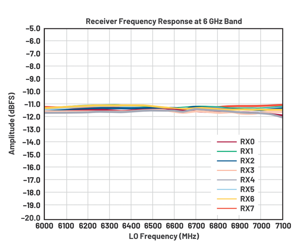 Figure 4. Receiver frequency response at 6 GHz band.
Observation receiver
In this highly integrated transceiver, two observation receivers are designed as the RF sampling architecture, which provides performance for the loopback receiver of the DPD for the power amplifier, the monitoring path for the transmitter output power, or the sniffing receiver for the RF spectrum, with appropriate front-end design.
To support the various applications, the observation receiver can be configured to work at four sampling clock rates, which provides the flexibility to choose between bandwidth, NSD performance, and power. Table 1 shows the NSD performance and power at the different sampling clock rates.
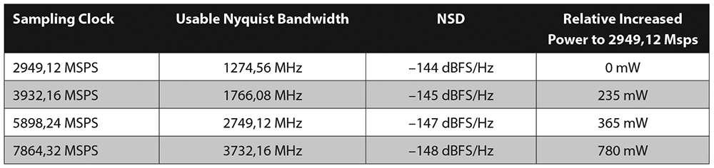 Table 1. NSD performance and power at different sampling clock rates.
Conclusion
In the wireless communication market, with the new technologies and the new spectrum continuously being adopted, a cost-effective solution is required as well by the operators. Therefore, a high integration and low power solution becomes more important. ADI’s 16 nm transceiver family integrates the eight channels with the high performance analogue front end, as well as the digital front-end functions on a single chip. The zero-IF architecture provides a low power transceiver solution, and the power saving feature (DTX) is integrated into the device to further reduce the system power consumption by controlling the PA. Its flexible configuration makes it an agile solution for a wide range of applications.
| Tel: | +27 11 923 9600 |
| Email: | [email protected] |
| www: | www.altronarrow.com |
| Articles: | More information and articles about Altron Arrow |


© Technews Publishing (Pty) Ltd | All Rights Reserved
 printer friendly version