


Over the past few years there has been a lot of discussion over the need for higher temperature materials and expanding the use and knowledge of high temperature assembly techniques. When we start to talk about high temperature electronics it is not just the solder alloy but all of the materials that go to produce an electronic assembly. Substrates, components, connectors, cables and solder need to be examined, and the needs of the assembly process also require careful consideration.
Often, due to the smaller volumes, many companies who require high temperature capability have used manual soldering techniques, particularly for through-hole with robotic soldering as an option. Working at high temperature generally means operating between 150-200°C; however, there are many applications that have to work at much higher levels, up to 300°C. Typically the industries affected by these hostile working conditions include aerospace, automotive, petrochemical and military.
This project was undertaken to obtain a basic understanding of the impact of through-hole solder joints in high temperature applications after artificially ageing. The aim of this investigation was to get a better understanding of existing assembly methods and future soldering processes.
Although the industry has been using high melting point lead/tin solders for many years, there is limited information available. Generally there is limited reference to inspection criteria for soldering joints or the different process issues that may be experienced. The National Physical Laboratory (NPL) report [1] outlines in more detail the basic trials conducted and some of the important issues that must be considered during the design and assembly using different selective soldering techniques.

For high temperature operation up to 200°C there is basically one option for traditional organic laminate. Polyimide laminate construction has been successfully used for many years for high temperature operation, typically around 150-175°C. The solder mask material and the solder finish also need to be considered for this high temperature post-assembly environment. The most common surface finish selected for these applications is gold over nickel.
In many cases the assembly of products for high temperature applications are either small or medium volumes and can be successfully produced using manual soldering for through-hole applications. Automated point soldering or selective soldering may also be used if the quantity of products required is higher or a company wants to automate the process. In this project we have used manual soldering, selective, robotic tip and laser soldering to produce sample joints with different alloys.
The solder wire flux cores in existing high temperature products were formulated many years ago and are not necessarily optimised to leave a low volume of residue on the surface of the board. The materials do work successfully but they would not be considered low residue. Existing suppliers offering High Melting Point (HMP) alloys and silver antimony (Sn95/Sb5) leave a lot of flux residues.
Solder alloys used during the trials:
• Tin/copper/nickel (Sn-0.7Cu) at 227°C.
• Lead/tin/silver (Pb93-Sn5-Ag2) at 296-300°C.
• Tin/silver (Sn-3.5Ag) at 221°C.
• Tin/silver/copper (Sn-3.8Ag-0.7Cu) at 217-221°C.
• Lead/tin (Pb980-10Sn) at 268-302°C.
It is worth mentioning that depending on which industry you work in, the meaning of HMP solder can vary. It is always important to check the alloy in question rather than just assume that HMP means lead/tin or lead/tin/silver.
The soldering and de-soldering process with higher melting point wires still follows standard good practice procedures but at some point manual soldering cannot achieve the ideal joint. The first step is to consider pre-heating the product for either initial soldering or rework. These practices have already been successfully used with standard lead-free alloys like SnCu, SAC and lead based HMP solders. However, the high lead based alloys do need more practice to get the process right.
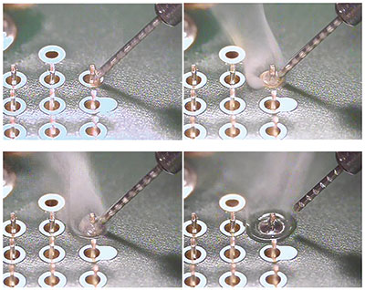
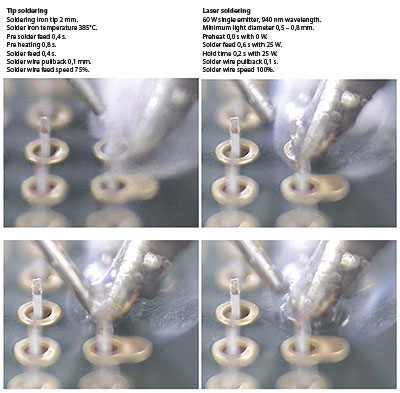
The robotic iron soldering system is basically a fully automated soldering iron with computer controlled parameters, programmed manually or by importing PCB design files. The systems are either three or four axis robots with either proprietary soldering heads and wire feeder systems or units that have been integrated with commercially available heads. This can also be the case for laser systems.
Robotic soldering has started to become more popular in recent years, with high reliability and automotive manufacturers trying to reduce the use of manual soldering. It has also been used in high volume production where a small number of joints need to be produced on each assembly, making it more viable than selective wave or jet soldering. It is clear that the sample board and connector used in this trial are more suited to a selective wave soldering process, but the speed of soldering was not necessarily part of this assessment.
As with any other printed board assembly, a product should be designed for manufacture rather than adapted to suit a process. One of the key features is accurately and repeatedly locating the product for the soldering operation, even if some form of vision alignment is provided.
Fixturing of the product for the soldering operation is very important for repeatability. If the product is a single board assembly then tooling or a fixture nest will be required for multiple boards if tip or laser soldering processes are to be used. If the boards are still in a multi-panel then standard tooling can be used, but the panel must be supported to prevent sagging and inconsistent height. Some equipment has automatic height sensing to deal with sagging or warpage of boards.
It is very important to define the process parameters used for soldering and determine their repeatability during trials. Through-hole fill is the key parameter in terms of inspection and in process quality control, but inspection of the board, copper plating, laminate, pad and solder mask are also important.
Sample joints were cut from the printed board for microsectioning. Measurements of the intermetallic thickness were undertaken on each of the samples. The majority of the samples prior to ageing provided intermetallic thickness of <1 µm. One sample showed measurements of 1-2 µm. This sample was produced with laser on tin/copper alloy but is not considered to be significant.
The average results of the measurements are recorded below after 1000 hours; they ranged from 5 µm to 16 µm.
• Sample 1. Tin/antimony hand soldered: 5 µm.
• Sample 2. Tin/antimony selective soldered: 10,5 µm.
• Sample 3. HMP selective soldered: 16 µm.
• Sample 4. SAC laser soldered: 8,5 µm.
• Sample 5. SAC robotic iron soldered: 8,1 µm.
• Sample 6. Tin/copper/nickel laser soldered: 9,2 µm.
• Sample 7. Tin/copper/nickel robotic iron soldered: 8,4 µm.
The outcome of the trials has been a better understanding of the results that can be obtained from the use of robotic soldering with different alloys, plus seeing some of the process challenges that can be experienced in manufacture and how to overcome them.
References
[1] Practical Guide to Soldering PCBs with High Temperature Solder Alloys, NPL Good Practice Guide No. 136, http://eprintspublications.npl.co.uk/6569/






© Technews Publishing (Pty) Ltd | All Rights Reserved
 printer friendly version