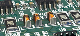
A new vision technology from Mycronic is bringing faster cycle times and higher resolution to 3D automated optical inspection (AOI).
Rapid electrification is causing a massive change within the electronics manufacturing industry. From electric vehicles to industrial robotics to power control systems, the world is witnessing the rollout of advanced electronics each more specialised and advanced than the previous. Manufacturing processes require the highest levels of quality, reliability and consistency to produce these advanced circuits. The latest vision system from Mycronic achieves a faster, sharper, and smarter path towards this goal.
The company’s latest contribution to this effort is aimed at the heart of one of its key limiting factors: the speed and accuracy of 3D AOI inspection. With its new Iris 3D AOI vision technology, it’s now possible to achieve the industry’s highest resolution 3D image capture at cycle times up to 30% faster than with previous inspection systems.
“To be clear,” explains Alexia Vey, product manager at Mycronic, “this is a speed increase of 30% for the full inspection cycle, from image acquisition to processing. Considering the system also handles nearly twice as many pixels, this is quite a remarkable performance improvement.”
Key to enabling this next-generation Iris technology is a range of best-in-class laser scanners, image sensors, lighting and computing systems. To expand the system’s field of view by 33%, a faster 3D laser sensor has been combined with improved telecentric optics. When it comes to resolution, the Iris system includes a new image sensor capable of capturing pixel sizes of 13,7 µm, resulting in an astounding 3,45 µm XY measurement resolution using sub-pixel technology. Together, these and other enhancements amount to a combination of speed, accuracy and coverage that is unmatched by any other system on the market.
Iris integrates a new generation of more powerful graphic processors, together with more efficient 3D construction algorithms. This increased processing allows the captured images to be processed at manufacturing takt time. As a result, the system achieves a wider test coverage and enhanced review images for components as small as 008004/0201M.
Iris 3D AOI vision technology is available as standard on all new MYPro I series 3D AOI systems. It is also available as a retrofit kit for existing K series 2D AOIs in need of an upgrade to 3D, as well as for K series 3D AOIs that demand improved processing speed.
World-first 016008 mm component placement
Manufacturing / Production Technology, Hardware & Services
Fuji has achieved the world’s first placement of 016008 mm (0,16 x 0,08 mm or 006 x 003 inches) size components on printed circuit boards with its SMT pick and place machine, NXTR.
Read more...Lifecycle and obsolescence: Protecting electronics through process Production Logix
Manufacturing / Production Technology, Hardware & Services
At Production Logix, we believe longevity is not accidental. It is engineered through early visibility, structured response, and disciplined execution, in partnership with our OEM customers.
Read more...Maximising squeegee quality and durability Testerion
Manufacturing / Production Technology, Hardware & Services
Transition Automation has announced two new product advancements designed to improve SMT printing performance and extend squeegee life: laser-enhanced Permalex bonding and integrated edge protectors.
Read more...NeoDen ND2 PCB screen printer ZETECH ONE
Manufacturing / Production Technology, Hardware & Services
The NeoDen ND2 PCB screen printing machine is a fully automatic stencil printer designed to deliver precise and consistent solder paste application in modern SMT production environments.
Read more...Understanding the BGA rework process Techmet
Manufacturing / Production Technology, Hardware & Services
BGA rework is a highly technical process that involves removing the faulty component, preparing the circuit board, and installing a new or repaired device, while maintaining the integrity of the printed circuit board.
Read more...Flexible three-process reflow soldering system Truth Electronic Manufacturing
Manufacturing / Production Technology, Hardware & Services
By combining multiple soldering technologies within a single system, the Vision TripleX system enables manufacturers to adapt easily to different assembly requirements, board designs, and production volumes.
Read more...Inline vapour phase soldering for high-volume production MyKay Tronics
Manufacturing / Production Technology, Hardware & Services
The VP2200-100 vacuum inline vapour phase soldering system from ASSCON is designed for fully automated, high-volume electronics manufacturing where process consistency and solder joint quality are critical.
Read more...Global electronics solutions since 1964 IMP Electronics Solutions
Manufacturing / Production Technology, Hardware & Services
Over more than six decades, IMP Electronics Solutions has built a reputation for technical expertise, reliable supply chains, and strong partnerships with both customers and manufacturing partners.
Read more...Driving excellence in electronics manufacturing Jemstech
Editor's Choice Manufacturing / Production Technology, Hardware & Services
Jemstech’s reputation for disciplined execution and client-focused service has earned it strong loyalty from companies operating in demanding industries.
Read more...When do you need Nitrogen in reflow? Truth Electronic Manufacturing
Manufacturing / Production Technology, Hardware & Services
Nitrogen in reflow soldering is often seen as a performance enhancer, offering improved wetting, shinier joints, and fewer defects. But it is not always necessary.
While every effort has been made to ensure the accuracy of the information contained herein, the publisher and its agents cannot be held responsible for any errors contained, or any loss incurred as a result. Articles published do not necessarily reflect the views of the publishers. The editor reserves the right to alter or cut copy. Articles submitted are deemed to have been cleared for publication. Advertisements and company contact details are published as provided by the advertiser. Technews Publishing (Pty) Ltd cannot be held responsible for the accuracy or veracity of supplied material.


 printer friendly version