Driving an ADC for an optimum mixed-signal performance is a design challenge. Figure 1 shows a standard driver-ADC circuit. During ADC acquisition time, the sampling capacitor sends back an exponentially decaying voltage and current into the RC filter. A mixed-signal ADC driver circuit’s optimum performance depends on multiple variables. The driver’s settling time, the RC filter’s time constant, driving impedance, and the ADC sampling capacitor’s kickback current, all interact during acquisition time and contribute towards sampling errors. These sampling errors increase directly with the number of ADC bits, input frequency, and sampling frequency.
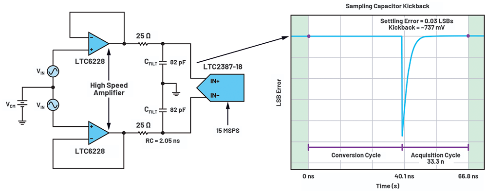 Figure 1. A standard ADC driver and RC filter.
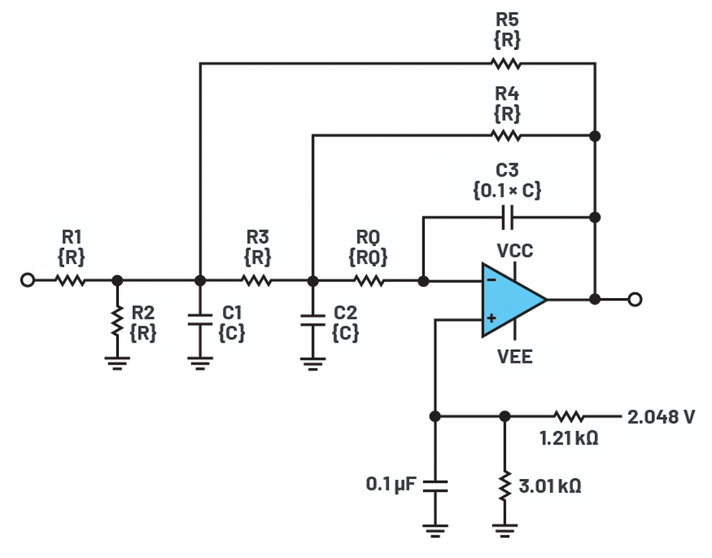
The standard ADC driver has a large sample of experimental data to use for a reliable design procedure. However, there is a lack of lab data to guide the design of a low-pass filter that drives an ADC. This article features an LPF driver circuit that combines analogue low-pass filtering, signal compression, and an ADC driver (see Figure 2). The cut-off frequency can be varied by changing either R or C in the circuit.
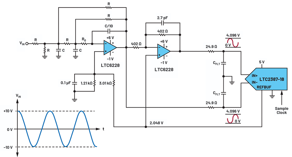 Figure 2. An LPF driver and ADC circuit.
The RQ resistor of the LPF sets the time response. A higher RQ has higher overshoot and longer settling time. A lower RQ has lower overshoot and shorter settling time. Figure 3 shows the LPF transient response for a 150 Ω and 75 Ω RQ resistor.
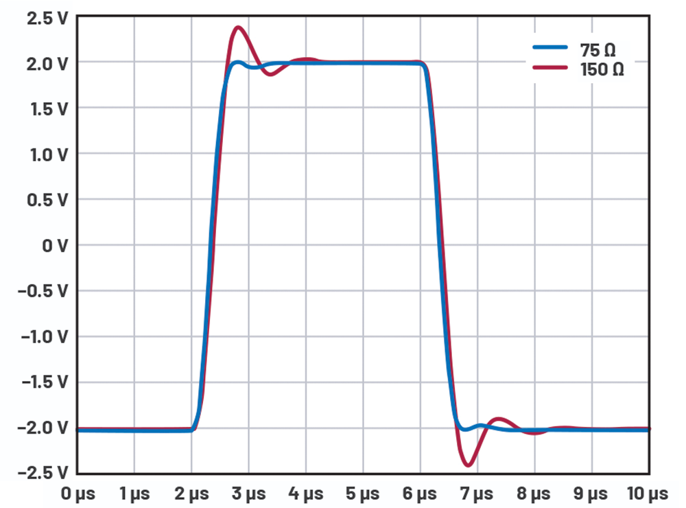 Figure 3. Overshoot and settling time for different RQ values.
Based on measured data shown in Table 1, using RQ of 75 Ω and 150 Ω has no significant impact on the SNR and THD performance and is only a factor for overshoot and settling time.
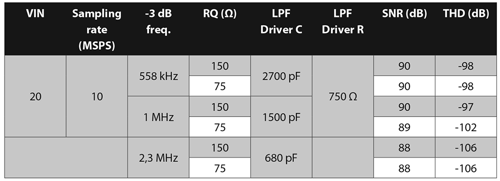 Table 1. LPF driver performance for different RQ values.
ADC sampling rate
The data in Table 2 shows that the THD performance of the system is lower using LTC2387-18 at 10 MSPS than 15 MSPS.
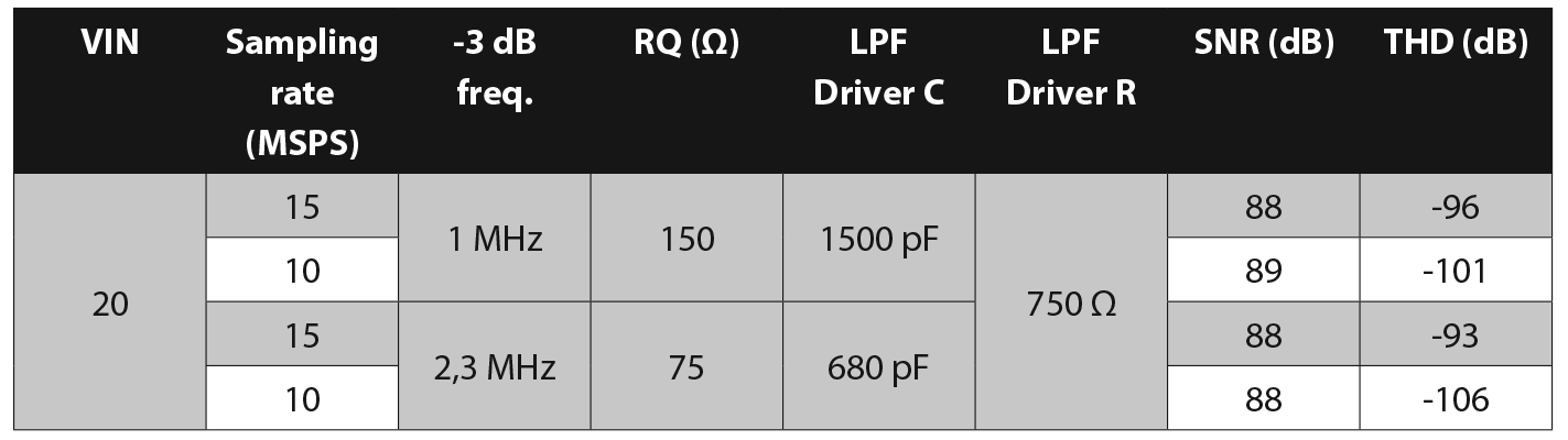 Table 2. LPF driver performance for 10 MSPS and 15 MSPS sampling rate.
RC filter
The RC filter between the driver and the ADC is used for bandwidth limiting to ensure low noise over wide bandwidth and to get better SNR. The RC value determines the –3 dB cut-off frequency. Lowering R can sometimes result in ringing and instability. Increasing R increases the sampling error. Using lower values for C will result in higher charge kickback but will allow faster charging time. A higher C value will give lower charge kickback but will also result in slower charging time. In addition, setting the values of RC is critical to ensuring that the sample is settled within the given acquisition time.
Using the data sheet’s recommended value and the suggested value from the Precision ADC Driver Tool is a useful starting point. The Precision ADC Driver Tool is a comprehensive tool that can help to predict system performance when using different RC values between the driver and ADC.
To achieve a lower –3 dB cut-off frequency by using 25 Ω and 180 pF for RC, the settling of the input signal and the charge kickback are affected. To have a lower –3 dB cut-off frequency, and to ensure the input signal is properly settled within the acquisition period, using a lower sampling rate can be an option. From the LTC2387-18 data sheet, the acquisition time is typically cycle time minus 39 ns. Optimising the LTC2387-18 at 15 MSPS results in a 27,67 ns acquisition time, while using this part at 10 MSPS results in a 61 ns acquisition time.
Amplifier driver selection
Best specifications for optimum performance of the parts are critical in the selection of ADC driver to be used. Two ADC drivers have been used on data gathering, the ADA4899-1 and LTC6228. These ADC drivers are good options for driving the LTC2387-18, which has been used for lab measurements. Some of the specifications that have been considered in the selection of the ADC driver are the BW, voltage noise, harmonic distortion, and the current drive capability. Based on the tests done, in terms of THD and SNR, the ADA4899-1 and LTC6228 have a negligible difference in performance.
LPF design and application guide
Figure 4 shows the LPF circuit. Five equal resistors (R1 to R5), one resistor (RQ) for adjusting LPF time response, two equal capacitors to ground (C1 and C2), and a feedback capacitor (C3) that is one-tenth the value of a grounded capacitor, complete the set of the LPF passive components (±1% resistors and ±5% capacitors).
A simple LPF design procedure
R1 to R5 = R, C1 and C2 = C.
For minimum distortion, resistors R1 to R5 must be in the range 600 to 750 Ω.
• Set R = 750 Ω.
• C = 1.5E9/f3dB nearest standard 5% capacitor in pF, f3dB is the LPF –3 dB frequency. For example: If f3dB is 1 MHz, then C = (1,5E9) / (1E6) = 1500 pF.
• C3 = C/10.
• RQ = R/5 or R/10 (see following note).
Note: RQ = R/5 for maximum stop-band attenuation or R/10 for low overshoot and fast settling. For RQ/5 and RQ/10, the stop-band attenuation is –70 dB and –62 dB, respectively, at 10× f–3dB. If RQ = R/10, then the –3 dB frequency is 7% lower than for RQ = R/5, so R1 to R5 is 0,93× the R for RQ/5.
Conclusion
The SNR and THD data provide insight into the performance of the circuit shown in Figure 2. Lowering the LPF bandwidth by increasing capacitors increases the SNR (lower LPF noise BW). A lower LPF bandwidth increases distortion (because the LPF settling time is longer than required for minimum sampling errors). In addition, if the LPF resistors values are too low, then the THD decreases because the LPF op amp drives the feedback resistors and the inverting op amp input resistor (at a higher op amp output current, distortion increases).
Using a 10 MSPS sampling frequency for the LTC2387-18 ADC, the LPF pass band must be 1 MHz or higher to minimise THD. Setting the LPF at 1 MHz is an arbitrary compromise for SNR, THD, and adequate ADC aliasing protection.
| Tel: | +27 11 923 9600 |
| Email: | [email protected] |
| www: | www.altronarrow.com |
| Articles: | More information and articles about Altron Arrow |


© Technews Publishing (Pty) Ltd | All Rights Reserved
 printer friendly version