

The world is currently in the midst of a solar revolution. In 2022 solar photovoltaics (PV) accounted for 4,5% of the total global electricity generation, with 1310 TWh being produced. This amounted to a 21,7% growth over the previous year.
Everyone knows that solar generation converts sunlight to electricity, but what comprises a solar panel, and how do they actually work?
The overall materials that make up a solar panel do differ between manufacturers, but they all have certain materials in common. Solar panels are made up of many solar cells connected to form a grid of cells or an array. The most popular choice of material in these cells is silicon in the form of a crystalline structure. Crystalline silicon (c-Si) can be separated into different categories based on the crystal size of the resulting silicon wafer used in the cell, with the two most popular categories being Polycrystalline silicon and Monocrystalline silicon.
A less popular choice for solar panels uses thin film cells. These panels tend to be cheaper, but they do not have the performance of the c-Si technology. One benefit of thin film cells is that they are flexible and therefore offer more durability especially for mobile applications.
How do these cells functions?
Each solar cell is made up of two types of semiconductors, a p-type (positive) and an n-type (negative), both of which are silicon-based. The p-type semiconductor is produced by adding atoms that have one less electron in their outer energy level than silicon has. The material used in this process is typically boron or gallium. This creates an electron vacancy or ‘hole’, which creates a positively charged area.
The n-type silicon is produced by including atoms that have an extra electron in their outer level compared to silicon. To create this, phosphorus is typically bonded to the silicon, as phosphorus has five electrons in its outer level. When the phosphorus bonds with the silicon, four of its five electrons are used. The fifth electron, however, cannot bond, and is therefore free to move into the silicon structure.
These two silicon layers, the n-type and the p-type, are sandwiched together. The excess electrons in the n-type silicon layer can then move across to the positively charged holes in the p-type silicon layer. This creates an area around the junction of the two layers called the depletion zone.
When all the holes in the depletion zone are filled with electrons, the p-type side of the depletion zone now contains negatively charged ions, and the n-type side contains positively charged ions. The presence of these opposing charges creates an internal electric field across the silicon layers.
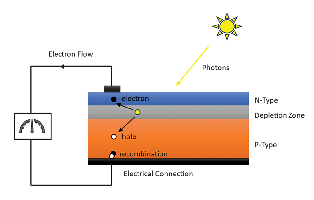
When a photon (from incident sunlight) strikes one of these solar cells, an electron in the silicon is emitted, resulting in the formation of a hole – this is known as an electron-hole pair. The electric field then has the potential to move electrons to the n-type layer and create holes in the p-type layer.
If a metallic connection is made between the p- and n-type layers, when photons strike the cell, electrons will travel from the n-type layer through the depletion zone to the p-type layer, and then travel through the external circuit connection back to the n-type layer (figure 1). This movement creates the flow of electricity across each cell, with each cell typically producing approximately 0,46 V DC.
These cells are arranged in a series configuration in a solar panel. Depending on the physical size of the panel, the number of cells vary between 32, 48, 60, 72 and 96 in a configuration. Therefore, a panel comprising 72 cells will generate a voltage of
Monocrystalline vs polycrystalline
In monocrystalline panels, the cells are produced using a single silicon crystal, which is grown under clean conditions in a controlled environment. The silicon is cut into wafers or discs and then shaved into the shape of an octagon. This allows one to fit more wafers into a smaller area.
Single crystals result in a higher quality of solar panels with a higher efficiency, resulting in more power being generated. However, the manufacturing process is expensive, and much of the silicon material is wasted during the shaving process. This results in a panel that is more expensive than the polycrystalline panels.
Polycrystalline panels are made up from multiple fragments of silicon crystals, which can also include the excess waste from the manufacture of monocrystalline panels. The silicon fragments are melted together and then cooled to form a polycrystalline structure. This polycrystalline material is then cut into wafers for the manufacture of solar cells.
Using silicon fragments in the manufacture of cells means that the material can never be ‘pure’ as it will have imperfections in its structure. This results in cells with reduced efficiency. However, because the silicon wafers are easier to produce and the excess material from monocrystalline production can be reused, the cost to manufacture polycrystalline cells is lower.
In a direct comparison, monocrystalline panels have an efficiency of 15 to 23% compared to 13 to 17% of polycrystalline panels. Mono panels are also smaller in size for the same output and therefore require less physical roof space. Mono panels have a lower temperature coefficient, meaning that they are more efficient in hot climates compared to their polycrystalline counterparts.






© Technews Publishing (Pty) Ltd | All Rights Reserved
 printer friendly version