


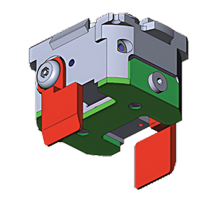
In telecom infrastructure and data centres, switches and server cards are adopting custom processors to satisfy demands for compute-hungry services and AI acceleration. Today’s largest adaptive FPGA compute engines are housed in BGA packages up to 55 x 55 mm, and multi-chip ASIC processors can be significantly larger, especially with fan-out interconnects.
Automotive electronics are scaling too, as embedded systems require increased current delivery for more powerful processors, expanded I/O to handle camera, radar, lidar, ToF, and inertial sensing channels. Control systems need larger connectors to handle extra data channels and power, and large bottom-terminated packages such as BGAs – avoided in the past due to inspection challenges – are now being adopted out of necessity.
The challenge to manufacturing
Equipment manufacturers serving these markets need to be able to place large and heavy components accurately and at high speed and high yield. It calls for reliable and secure pick-up from trays or pallets, rapid positioning, and accurate alignment before placing the component. Through-hole parts like some types of connectors and transformers need a reliable solution for press fitting. The components can be large, tall, and bulky, while assembling press-fit components calls for accurate pin alignment before insertion. Historically challenges like these, involving such large components, have exceeded the typical capabilities of regular surface-mount placement equipment.
An inline solution is preferable, to help assemblers maintain efficiency and productivity. Better still, using standard surface-mount machines to place large BGAs and press-fit connectors saves investing in special equipment or performing operations such as assembling connectors offline.
Flexible placement
Engineering a solution for placing large and heavy components at speed demands some critical changes to standard mounters. Adaptations to the placement head are among the most important.
Gripper nozzles that combine suction with claws are extremely effective for holding unusual components securely. Until now, procuring nozzles like this has required assemblers to engage with their equipment suppliers to design a custom gripper. But, as larger and heavier IC packages and connectors, as well as inductors, transformers, and power components are more widely used, gripper nozzles can no longer be regarded a specialist item. A more efficient approach is needed.
Standardising the claw and backing-plate designs relieves the time and cost pressures that come with a custom engineering project. Yamaha Robotics has standardised a range of claws and backing plates that allow 60 different configurations to handle various component types and sizes. Choosing a suitable combination lets manufacturers scale their component-placement capabilities quickly and easily.
On the other hand, rubber pad nozzles can provide an affordable and effective way to pick up large ICs by applying suction directly to the package upper surface. Yamaha is developing rubber nozzles in a variety of sizes up to 25 mm diameter for lifting the heaviest components. Part-specific nozzles designed for picking up components such as DIMM memory module expansion sockets for server cards are also in development.
Before placement, the component must be correctly oriented by rotating the nozzle. When placing small and lightweight components, the R-axis motor can drive the nozzle directly at high rotational speed. In contrast, the greater inertia associated with large and heavy components demands more careful motion control to prevent the component detaching from the nozzle. Although a reduction gear driven from the motor is an obvious solution, backlash in conventional gearing systems can impair accuracy. Yamaha’s scissor gear is specially designed to prevent backlash and permits aligning components like BGA ICs to within 0,005°.
To handle taller components, increasing the z-axis stroke by just a few millimetres can significantly expand the range of parts that can be handled. An extended stroke 40 mm is enough to let the machine handle today’s tallest automotive connectors.
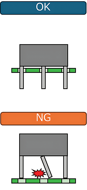
The machine-vision and lighting systems used to check for alignment must also be improved. The standard LED-based lighting systems typically used for component checking and alignment tend to illuminate the component body and the entire length of each pin, or lead, equally. Under these conditions, the vision system can struggle to distinguish the pin tip accurately to assess the readiness for insertion. A laser system can provide controlled and directional lighting to selectively illuminate only the pin tips and thus enable the vision system to verify that all pins are correctly aligned with their respective holes to allow insertion to go ahead.
In addition, to withstand the increased placement force and maintain positional accuracy, the underlying board support structure and push-up pin mechanism must also be strengthened.
Head-mounter interface
Yamaha designed its latest LM placement head to handle larger ICs, taller components, and more challenging press-fit parts, as well as placing SMD chips and other small components at high speed. Special features in both hardware and software implement extended R-axis control, Z-axis control, placement-force control and landing detection. New nozzles and a specially designed gripping section cater for larger components, and users can continue to attach their existing nozzles for placing parts in ordinary SMD, SOP, and QFP packages. A new nozzle health check feature lets users automate periodic inspection and cleaning and thereby ensure regular and adequate maintenance to maximise end-of-line yield and avoid unplanned downtime.
The LM head fits to YRM mounters using the same interface as other heads. On the other hand, new feature-recognition software for the YRM multi-camera increases the maximum recognisable IC-package size from 55 to 130 mm, and the maximum number of BGA balls from 4000 to 20 000. This is an important enhancement that lets the system recognise and align large FPGA and ASIC packages.
| Tel: | +27 31 822 8555/6 |
| Email: | [email protected] |
| www: | www.truthelectronics.co.za |
| Articles: | More information and articles about Truth Electronic Manufacturing |


© Technews Publishing (Pty) Ltd | All Rights Reserved
 printer friendly version