Editor's Choice


A new era in wire bond inspection

31 October 2025 Editor's Choice Manufacturing / Production Technology, Hardware & Services

As electronic assemblies become more compact and performance demands rise, wire bonding has grown increasingly complex. Industries such as automotive electronics and 5G communications now rely on ultrathin wires, finer pitches, and higher power capacities. These advances place new pressure on inspection processes to ensure absolute reliability and detect defects that could compromise safety or performance.

Traditional inspection approaches are no longer adequate. Electrical testing, for example, cannot verify whether multiple bonds are fully intact or determine the integrity of adhesive contact surfaces. Likewise, conventional 2D optical inspection systems lack height information, making it impossible to assess critical dimensions such as loop height, wedge elevation, wire clearance, or exact wire length.

Some manufacturers have attempted to adapt 3D inspection technologies used in SMT, but these are limited. Reflective, rounded bond wires, especially those under 300 µm, do not reflect sufficient usable data with systems originally designed for flat SMD components. As a result, key defects and dimensional inaccuracies often go undetected.

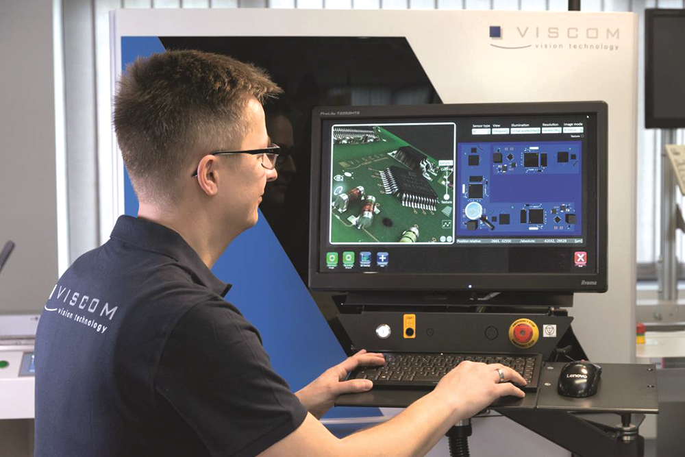
Recognising this gap, Viscom has developed a new 3D wire bond inspection solution tailored specifically to the unique challenges of wire bonding. The system incorporates a custom lighting concept, a proprietary camera setup, and a high-speed 3D imaging method.

At the core is a dome-style illumination system that combines reflected-light and dark-field techniques. This enables accurate imaging of shiny, slender wires, including those as thin as 15-20 µm. The custom camera provides 25-megapixel resolution and a high data transfer rate, which improves image quality and reduces false alarms. For 3D reconstruction, the system rapidly captures a stack of high-resolution 2D images and calculates the height profile using both CPU and GPU processing. This parallel processing enables full 3D inspection in-line without slowing production.

The platform accommodates various materials such as aluminium, copper, gold, silver, and ribbon or thick wire formats. Inspection covers bond positions, wire routing, dies, and component placement, while inspection programs can be created offline to avoid production interruptions.

A built-in classification and statistical process control station adds another layer of value. Defect candidates can be reviewed and categorised, and trend analysis tools help identify recurring issues. Typical findings include misaligned die attachments, missing or malformed balls or wedges, wire breaks, pinched routes, and incorrect spacing or loop shapes. The system can also detect changes caused by tool wear, contamination, or parameter shifts after maintenance.

One of the major breakthroughs is the ability to measure true wire and wedge heights. Minimum clearances, loop elevations, and precise wire lengths can now be verified, which is especially beneficial in tightly packed assemblies. Even wafer indentation depth in ribbon bonds can be fully assessed – something that was previously impossible to perform in-line.

By combining high-resolution 2D imagery with accurate 3D data, the system significantly reduces false calls, while improving inspection speed. This hybrid approach ensures that complex assemblies can be inspected thoroughly and efficiently, supporting better quality control and more stable production processes.


Credit(s)


Share this article:
Share via emailShare via LinkedInPrint this page

Further reading:

Quectel’s RG255C-NA and RM255C-GL accelerate 5G RedCap adoption
iCorp Technologies Editor's Choice Telecoms, Datacoms, Wireless, IoT
Quectel’s RG255C-NA and RM255C-GL modules represent a strategic move into this fast-growing segment, delivering Sub-6 GHz 5G connectivity optimised for mid-tier IoT applications.

Read more...
SDRs – Which RF architecture should you choose?
RFiber Solutions Editor's Choice Telecoms, Datacoms, Wireless, IoT
There are several common methods of implementing SDR architectures. This paper discusses which is best when meeting a specific need.

Read more...
Surviving the extremes: Understanding shock and vibration in MEMS sensors
Altron Arrow Editor's Choice Test & Measurement
By considering factors such as mechanical headroom, damping, and system-level robustness, designers can ensure that the chosen sensor not only survives, but performs reliably over time.

Read more...
A two-stage approach to super-wide input voltage range DC-DC converters
RFiber Solutions Editor's Choice
Teaser: In addition to handling the various input voltage ranges required, the SynQor line of InQor DC-DC converters are fully encased and ruggedised to handle the harsh environments that often accompany systems that have such challenging technical requirements.

Read more...
From the editor's desk: Engineering the future
Technews Publishing Editor's Choice
As we welcome the first issue of Dataweek in a new year, it is an exciting time to be part of the electronics community, especially for our readers. The pace of change across our industry continues to accelerate, reshaping how we design, build, and interact with technology.

Read more...
Barracuda commissions new IPC Class 3 aerospace facility
Barracuda Holdings Editor's Choice News
The company has commissioned a new dedicated IPC Class 3 facility in Somerset West. and has concluded a new investment partnership that will provide the capital and management capacity required to scale operations.

Read more...
Engineering copper grain structure for high-yield hybrid bonding in 3D packaging
Testerion Editor's Choice Manufacturing / Production Technology, Hardware & Services
The way copper grains are sized and distributed forms the metallurgical foundation of hybrid bonding, enabling lower bonding temperatures, greater reliability, and stable grain structures throughout integration.

Read more...
Understanding solder dross: causes and control strategies
Truth Electronic Manufacturing Editor's Choice Manufacturing / Production Technology, Hardware & Services
Dross formation is an inevitable consequence of wave soldering. It occurs when molten solder comes into contact with oxygen, forming metal oxides that float on the surface of the solder bath. Over time, this oxidation byproduct accumulates and must be removed to maintain solder quality and process consistency.

Read more...
UV curing oven for high-efficiency PCB production
Techmet Manufacturing / Production Technology, Hardware & Services
The jCURE-2UV+ from JTU is a cutting-edge ultraviolet curing oven engineered for fast, reliable curing of UV-sensitive coatings in SMT production environments.

Read more...
Automated X-ray inspection
Techmet Manufacturing / Production Technology, Hardware & Services
The SAKI 3D-CT AXI stands at the forefront of automated X-ray inspection technology, delivering excellent performance for SMT, through-hole, and semiconductor inspection processes.

Read more...


While every effort has been made to ensure the accuracy of the information contained herein, the publisher and its agents cannot be held responsible for any errors contained, or any loss incurred as a result. Articles published do not necessarily reflect the views of the publishers. The editor reserves the right to alter or cut copy. Articles submitted are deemed to have been cleared for publication. Advertisements and company contact details are published as provided by the advertiser. Technews Publishing (Pty) Ltd cannot be held responsible for the accuracy or veracity of supplied material.


© Technews Publishing (Pty) Ltd | All Rights Reserved