


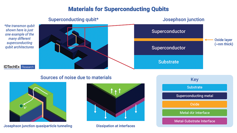
 Figure 1. Materials for superconducting qubits [source: IDTechEx Research].
Superconducting chips
Superconductivity is a phenomenon where certain materials exhibit zero resistivity when below a certain critical temperature. The behaviour of superconductors is fundamentally quantum in nature, so it is no surprise that some of the earliest work showing the macroscopic effects of quantum mechanics was performed using superconducting circuits, such as the work by Clarke, Devoret, and Martinis which was awarded the 2025 Nobel Prize in Physics.
Beyond academic accolades, quantum computers and quantum sensors built on superconducting chips have become a commercial technology. Superconducting qubit quantum computing is one of the oldest and most established qubit modalities (technological approaches to quantum computing). IBM has been championing the approach for over a decade and dozens of other players such as Google Quantum AI, Rigetti, and IQM are now following suit with their own technology stack and chip architectures.
Superconductors also underpin two important types of quantum sensors: SQUIDs and SNSPDs. Superconducting quantum interference devices (SQUIDs) can be used for extremely accurate sensing and imaging of very faint magnetic fields, such as those emitted by the brain in SQUID MEG (magnetoencephalography) machines. Meanwhile, superconducting nanowire single photon detectors (SNSPDs) represent the highest performance in single photon detection – the measurement of individual particles of light which is crucial for photonic quantum computing, quantum communications, and more applications beyond the quantum industry.
The need for nanometre fabrication precision
To achieve the scalable and repeatable production of superconducting circuits for quantum technology products, players in the industry are leveraging semiconductor fabrication techniques. In these processes, layers of superconducting material are deposited on semiconductor wafers (typically silicon, silicon dioxide, or sapphire) and then shaped into the required circuit patterns through various lithography and etching steps. The superconducting material used varies by player but is typically aluminium, niobium, or tantalum for superconducting qubits and SQUIDs, and often compounds such as niobium nitride (NbN) for SNSPDs.
However, superconducting chips face a very stringent challenge in precision. Both SQUIDs and superconducting qubits are based on a device called a Josephson junction. A Josephson junction is formed by having two pieces of superconducting material separated by a thin insulating barrier, which is thin enough (in the order of nm) to allow for quantum tunnelling. At temperatures below the critical temperature of the superconducting material, charges flow as Cooper pairs, which can tunnel through the insulating barrier at a material critical current dependent on the material, its temperature, and its dimensions.
The critical current of the Josephson is exponentially sensitive to the thickness of the insulating tunnel barrier. As a result, even angstrom-scale (~0,1nm) variations in the thickness of the deposited insulator material can yield variations of a few percent in the critical current, which in turn causes a few percent variation in the superconducting qubit frequency. Qubit-to-qubit variations in frequency can reduce the yield of the quantum chip or complicate operations.
However, the challenge does not stop there, recent work suggests that effects at material interfaces can cause noise and variations in qubit frequency. Microfabrication techniques that go beyond the current state-of-the-art are therefore required to produce high quality superconducting qubits at the scale required for commercial quantum computing. IDTechEx’s full ‘Materials for Quantum Technologies’ report goes into more depth on the various solutions proposed by the industry including new fabrication and packaging methods, chiplet architectures, and automated diagnostics.
Market outlook
SQUIDs, SNSPDs, and superconducting quantum computing are some of the most mature and well-documented quantum technologies, however the work in improving the quality and scalability of superconducting quantum chip fabrication is far from over. Techniques that can consistently fabricate Josephson junctions to sub-nm-scale accuracy, while minimising defects and variations at material interfaces will be key to improving the coherence time and fidelity of qubits across the chip.
In the article ‘Materials for Quantum Technologies 2026 – 2046: Market, Trends, Players, Forecasts’, some of the challenges in fabricating superconducting chips for quantum computing and sensing is explored. The report comprehensively covers the material opportunities in the three main quantum market verticals (computing, sensing, communications), and in the most important material platforms (superconducting chips, photonics, and nanomaterials). This multi-dimensional analysis highlights the intersections between different products, illuminating key materials opportunities in the quantum industry, such as the need for more precise superconducting chip fabrication.
For more information visit www.idtechex.com/quantummats


© Technews Publishing (Pty) Ltd | All Rights Reserved
 printer friendly version