


It is common for IoT devices, industrial sensors, meters, and medical equipment to require both a positive and negative voltage. Often, these voltages must be symmetrical and sourced from a single power supply. This article explains the available options and technical requirements needed to produce a negative rail from a positive rail supply.
Various electronic designs require one or more negative voltages in the power supply, often coming together with a symmetrical positive voltage. Some typical application examples are:
• In gate drives for the charger and traction inverter of electric vehicles.
• In high performance ADC and DAC and rail-to-rail operational amplifiers for industrial and medical applications.
• In LCD displays.
• In driving photodiodes.
The following details two typical block diagrams of such systems.
Gate drivers
For high power SMPS and motor drives, a negative driving voltage is often required because:
• Systems may not have a tightly placed and coupled PCB layout, and its circuit ground usually couples with noise from the system and may fluctuate around ground level.
• The main power devices such as IGBTs, SiC, or GaN FETs are often placed up to centimetres away from the gate control circuitry unless they are all housed inside a module. Hence, the signal coming out of the gate drivers may be distorted as they reach the power devices, and the additional safety margin is desired.
• Advanced power devices such as GaN FETs often have a low turn-on threshold, making them more sensitive to gate voltage ringing. Some high voltage GaN FETs may have high CGD or wide process variation, which may cause a Miller effect-induced turn-on. In this case, the end customers are suggested to apply a negative gate voltage to ensure the device maintains its off status.
One example is using an isolated driver, ADuM4120. In such applications, the power devices are driven from positive voltage as in V1 and negative voltage as in V2, as seen in Figure 1.
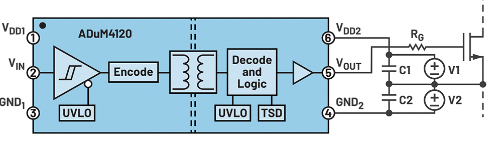 Figure 1. Example bipolar supply setup [Analog Devices].
Rail-to-rail op amps
For various signal conditioning applications, rail-to-rail op amps are often used where the output needs to have a wide span close to supply, the input swings around the reference, or when the highest precision is required. A typical example of a phono preamplifier system is shown in Figure 2. This design requires one positive 15 V and one negative 15 V.
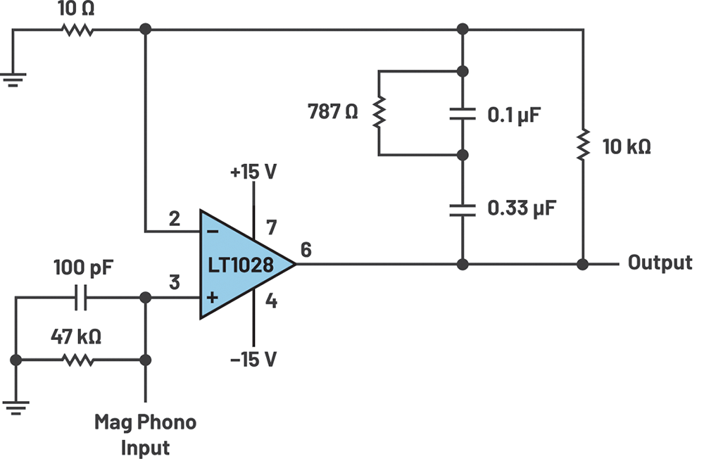 Figure 2. Typical application circuit of ultralow noise 1M TIA photodiode amplifier.
The solutions
The following solutions are listed in the order of complexity and general performance.
Zener diode
A simple way to generate ± voltages without an IC is to use a Zener diode, as shown in Figure 3. In this solution, the output of the V3 source is split by Dz and Rz. If V3 is 9 V and Dz is a 5 V Zener diode, then the gate will be driven by +5 V and –4 V. This method provides a low-cost solution as it does not require additional ICs. However, this solution is highly inefficient and is not suitable for applications that require tens of milliamps and a well-regulated output voltage. Hence, this topology is not often used.
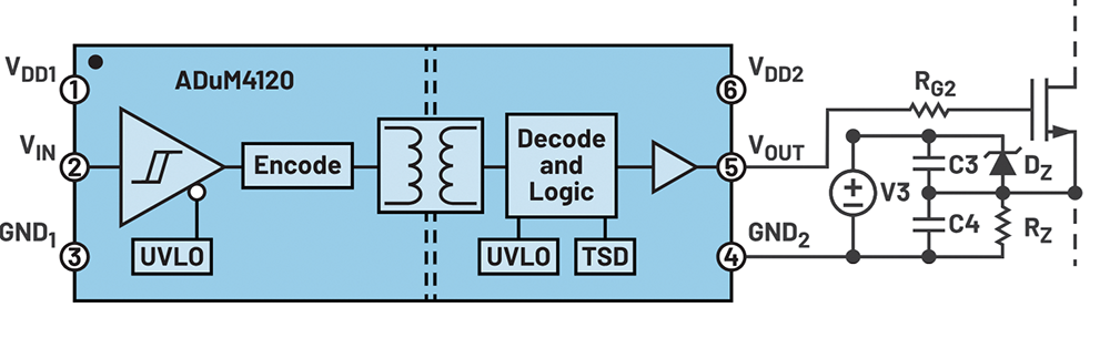 Figure 3. Negative voltage Zener diode rail example.
Charge pump
Using a charge pump is a convenient method to invert the positive input since no magnetic component is required. For low power needs, Analog Devices offers several regulated and unregulated charge pumps, like the LTC1983 in Figure 4. While this solution is very simple with a small form factor, the drawback is on efficiency, and possible high electromagnetic interference. This device category is limited on load current and is generally used in applications that need less than 100 mA.
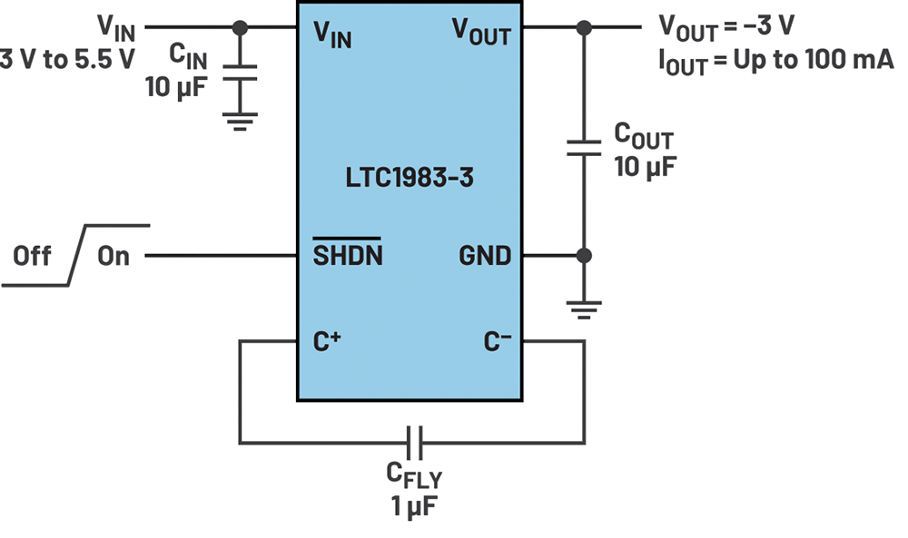 Figure 4. Typical application circuit of –3 V at 100 mA DC-DC converter.
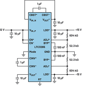
Alternatively, in the interest that low noise/low EMI is desired to avoid possible interference with other sensitive circuitry (especially for medical equipment, sensing, and communication applications), ADI offers products like the LTC3265 that integrates low noise LDO regulators to each of the dual charge pump outputs (Figure 5). While the output current is limited to 50 mA, this solution is much more EMI friendly and integrates both positive and negative output rails in just one IC. With very low output noise, it is helpful in precision instrumentation applications to drive low power op amps and data converters.
Inverting converter
Charge pumps are relatively more useful with known input/output combinations without accurate regulation needs, and the related noise interference is taken care of by additional filtering. For applications with a wide range of input or output voltages with tight regulation needs, it is recommended to use inductor-based switch-mode topologies.
There are a few such topologies that can handle positive to negative conversion, often all are categorised as inverting topologies and may confuse engineers. While they can often perform the same power conversion task, there are design compromises. Below are three typical topologies. The first two are similar; however, using a buck IC provides more options even though they are not specifically designed to generate negative voltages.
• Inverting buck-boost converter using a buck IC.
• Standalone inverting buck-boost converter.
• Dual-inductor inverting buck-boost converter.
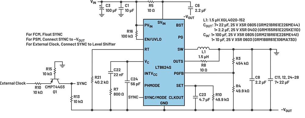 Figure 6. An IBB converter using the LT8624S buck IC.
Inverting buck-boost converter using a buck IC
When a typical synchronous buck converter’s output side is switched with circuit ground, an inverting buck-boost (IBB) converter is created, as shown in Figure 6. This approach is popular as there are many options for synchronous buck regulators or controllers available on the market. For noise-sensitive applications, ADI’s Silent Switcher monolithic buck regulators, such as the LT8624S using Silent Switcher 3 technology, can be configured as an IBB to generate a negative voltage rail with both excellent wideband and EMI noise performance. Figure 6 shows an example circuit of the LT8624S as an IBB. For further filtering, a low noise negative input LDO regulator can be added to the output.
The disadvantage here is the IC is referring to the buck converter ground, but not the system ground (which is the positive side of the output). If a microcontroller is needed to perform functions like enable, SYNC, or just receive a PGOOD signal, then an external level shifter circuit may be needed, which can be inconvenient. If PMBus/I2C communication is desired, then a level shifter may not work, and an external digital isolator IC may be necessary.
If a converter with no need for external sensing or control is used, then using a buck IC as an IBB is preferred, with a wider variety of options. All buck converters at any voltage and current ratings can be configured in this way, but most will need external level shifters to be controlled externally.
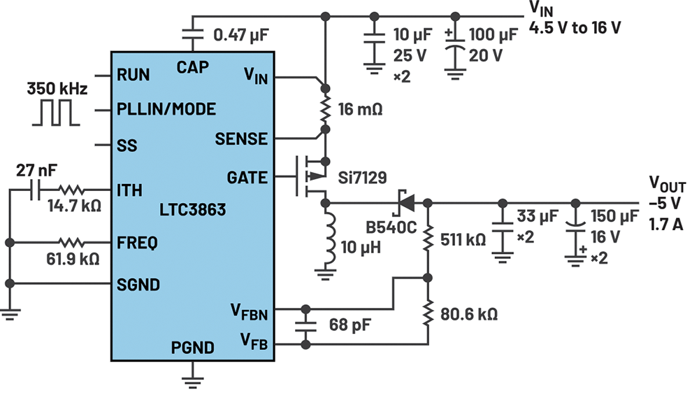 Figure 7. An asynchronous IBB converter.
Standalone inverting buck-boost converter
When external level shifters are not desired in the application, there are two solutions: use an asynchronous IBB, or integrate the level shifters into the buck IC. For example:
• Asynchronous IBB: An asynchronous IBB can be designed by using a PMOS as the primary switch and a diode instead of a synchronous switch. This allows the IC to be referenced to system ground without the need for level shifters. Here the positive side of the output load is tied to the input ground. The IC option here can be the LTC3863 as shown in Figure 7. It is often less efficient than using a buck IC because a PMOS and diode usually have more losses than an NMOS-based synchronous converter.
• Buck-based IBB with integrated level shifters: Instead of using external level shifters when using a buck IC as an IBB, each input and output signal can have its own level shifter integrated into the IC. This is convenient for designers. For example, the MAX17577/MAX17578 and MAX17579/MAX17580 are buck-based IBB converters that integrate level shifters at the EN and RESET pins. If high power and high efficiency are desired, then the LTC3896 is recommended. It is a more sophisticated, high performance synchronous switching controller with integrated level shifters, and is recommended for power requirements greater than 100 W.
Dual-inductor inverting buck-boost converter
When switching noise is a concern, a dual-inductor converter can generate a negative output voltage with less noise than an IBB converter. This topology is shown in Figure 8, with two inductors and one coupling capacitor. The advantage of this converter is in its simplicity: only a low-side switch is needed to invert the input, and it can be an NMOS so efficiency is high. For example, the LT8330 requires just 8 pins and is one of ADI’s regulators with two integrated error amplifiers that enable it to sense either positive or negative output voltage. Similar regulators such as the LT8331, LT8333, LT8334, LT8570, and LT8580 offer different ratings and features to cover a variety of common application requirements.
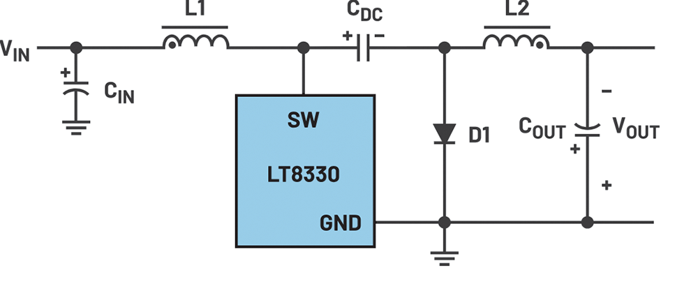 Figure 8. A simplified inverting converter.
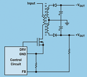 Figure 9. A typical flyback converter with multiple output windings.
While this topology does need two inductors, if the two inductors are coupled as shown in Figure 8, the output ripple is significantly reduced and may save on output capacitor size. Also, since one inductor sits on each input and output side, the currents are continuous, and the entire circuit can be less noisy than other topologies. If more power is desired, a controller IC with an external low-side FET, such as the LT3758 can be a good option.
Flyback converter
If a transformer is required for isolation purposes (like in a flyback converter), then it is very easy to create ± output voltages by adding another winding on the output side. Here on the transformer, by setting multiple windings in different directions, together with blocking diodes, a positive or negative voltage can be generated, as in Figure 9. For example, the LT8306 does not need an optocoupler for feedback, saving on bill of materials.
While convenient, the generated negative voltage is unregulated and if regulation is needed, it is recommended to add another negative input LDO regulator at the output.
Conclusion
Considering most applications that desire a negative output also require a complementary positive output, ADI has a variety of solutions that use the previously mentioned topologies and provide two or more dual-rail voltages within one IC. Examples include:
• Dual 42 VIN, 3 A boost/inverting regulator LT8582.
• Dual 50 VIN, 2 A multitopology regulator LT8471.
• Dual 5,5 VIN, 2 A/1,2 A boost/inverting regulator ADP5076.
• 3-channel 60 V isolated micropower management unit ADP1034.
For many engineers who desire an ultra-small solution or an off-shelf fully integrated power solution, a micro power module can be considered. For example, the LTM4655 is a 40 VIN, dual 4 A inverting μModule regulator, with two fully independent output channels, each configurable for positive or negative output, and is already EN550222 Class B compliant for low EMI performance. The LTM8049 is another good option, with up to 20 VIN, and two outputs, +24 V and –24 V.
| Tel: | +27 11 923 9600 |
| Email: | [email protected] |
| www: | www.altronarrow.com |
| Articles: | More information and articles about Altron Arrow |






© Technews Publishing (Pty) Ltd | All Rights Reserved
 printer friendly version