


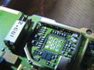
Micro ball grid array packages (µBGA) are rapidly becoming the package of choice when designing new printed circuit board (PCB) assemblies. These packages generally offer high, first-pass process yields with significant real estate savings over their predecessors.
Process or design errors occasionally require the need for rework. Because rework requires component removal, special considerations must be taken into account. These include excessive heat and improper removal as well as the fact that site-cleaning techniques have the potential to cause damage to component pads, adjacent components or the PCB itself. In short, proper rework requires sound practices, proper tools and quality training.
The following are some advantages to using BGA and land grid array (LGA) packages:
1. Higher I/O (input/output) density. As the drive to reduce board size continues, the need for greater I/O density intensifies. The fine-pitch μBGA package offers several times the amount of I/Os per unit area of PCB space than the widely used BGA.
2. Mechanically robust design. The μBGA can be handled without concern for bending and misaligning the leads. This reduces component packaging costs and pre-assembly defect rates of components.
3. More stringent placement tolerances. Standard BGAs typically offer a much larger pitch between terminals, making them more forgiving in terms of placement accuracy. The μBGA and LGA with their smaller ball size and lower pitch require more accurate placement. Typically, a machine with a placement accuracy of 1 mil is required. Likewise, the use of lead-free solders presents additional challenges, including decreased occurrences of self-centring during reflow and the inability to rely on the surface tension of the solder self-centring the device as in the past with standard, leaded BGAs.
4. Direct thermal path. In terms of heat dissipation from component to PCB, the LGA’s centre ground pad provides a direct path for heat to dissipate into the board. This reduces the thermal resistance of the interconnections, thus minimising the likelihood of damage to the chip and internal wire bonds.
5. Ease of stencil printing. The LGA makes the stencil printing process a requirement for rework since these components are supplied without solder. An LGA stencil plate must be designed to meet the requirements of the pattern and be fitted to the rework machine.
However, there are some disadvantages of the μBGA and LGA packages. First, solder joint integrity can be inspected only after reflow through the use of X-ray inspection, which is both time consuming and expensive. Second, the use of µBGAs involves a higher level of complexity in terms of signal trace routing on the PCB, adding to the cost of the board.
Finally, despite the high first-pass yields of the μBGA and LGA, defective solder joints still occur for various reasons. As a result, the rework process becomes more involved because solder joints are hidden and cannot be touched up and the component must be completely removed from the board. This requires rework equipment offering a higher level of process control.
Solder paste or flux deposition
With lead-free μBGAs, solder balls melt at 217°C and typically contain adequate solder volume to create an acceptable joint. Current industry trends are to apply paste flux during the rework operation; this will reduce the need for custom solder paste plates and provide the necessary flux for proper attachment. This can be best accomplished with a flux dip plate that ensures a consistent application of paste flux to the bottom 30% of the solder ball.
Conversely, LGAs require the application of the correct thickness of solder paste since the components are supplied tinned without adequate solder for connection to the PCB. In the case of rework, solder paste is applied with a single component stencil directly to the bottom of the component. The part is then picked from the component nest on the rework machine without disturbing the deposition of the solder paste.
During the rework of LGAs, solder paste volume is critical for long-term reliability. Stencil thickness and aperture sizes can be calculated for optimum solder volume. More specifically, manufacturers’ data sheets must be consulted for paste volume to ensure long-term reliability.
Placement
Featuring smaller ball sizes and finer pitches, BGAs and LGAs require more accurate placement. Typically, a machine with a placement accuracy of 1 mil is required. Likewise, as described above, use of lead-free solders presents additional challenges, including decreased occurrences of self-centring during reflow and the inability to rely on the surface tension of the solder self-centring the device as in the past with standard, leaded BGAs.
Reflow
The next significant concern associated with solder paste used in the LGA process is that of potential voids in solder joints caused by the flux material. Typically, these voids occur near the body of a LGA because the flux is lighter than the solder material, forcing it to rise to the top of the molten liquid ball.
Therefore, it is helpful to inform the paste vendor that LGAs are involved in the process, ensuring that the proper formulation of solder paste or flux can be recommended. Obviously, the proper application of an appropriate reflow profile minimises the possibility of voids. The reflow profile for LGA components is the same as for any surface mount device and the ideal reflow temperature is 235°C.
With μBGAs and LGAs, the nature of the defect types is quite similar to other SMT devices: solder bridging, cold solder joints or misalignment. In the case of defective joints, potential causes include defective solder balls, poor solder and/or flux quality, poor solder paste and/or flux deposition, unclean solder pads, or improperly applied reflow profiles. Misalignment, on the other hand, can be caused by a range of placement and handling problems.
Because the solder joints are inaccessible for single joint touchups and visual inspection, array devices are often the defect culprits on failed assemblies. Thus, it is critical that the rework process be carefully developed and performed with equipment that provides repeatable process control. The necessary rework process steps are:
1. Reflow (for removal)
2. Site preparation
3. Solder paste or flux deposition
4. Placement
5. Reflow
1. Reflow: The application of a uniform, repeatable reflow profile is crucial. The heating process must cause the full array of solder joints to achieve reflow simultaneously, yet in such a way that does not sacrifice the integrity of the component, the board or any adjacent components.
This is only achievable with a rework system that provides even heating on both the top and bottom sides of the board, with the heat flow contained within the space occupied by the device and applied in such a way that it minimises any temperature gradients across the component.
This calls for low-pressure convection airflow that heats through the body of the component. This should result in the simultaneous reflow of the joints that, combined with automatic vacuum part removal, reduces the probability of lifting pads off the board.
For each combination of PCB and array component, an appropriate reflow profile must be established. Careful profile setup is the key to successful reflow, and the proper placement of thermocouples during testing is critical to ensure uniform temperature across the component and the PCB assembly.
Board profiling must be done on a completely populated PCB with new thermocouples, a calibrated recording device and placement of the thermocouples in both high and low thermal demand areas of the board. The rework equipment should allow the operator to monitor temperatures beneath the component body as well as the output temperatures of the system’s heaters.
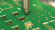
2. Site preparation: After component removal, the pads need to be prepared for the replacement component. The residual solder should be removed with a solder wick saturated with paste flux, used in conjunction with a direct power soldering iron equipped with a hot blade tip. The operator must be careful, keeping the wick between the tip and the board.
The old solder can be removed quickly without risking the pad damage that is likely to result from direct contact between a hot tip and the board. Subsequently, the flux residue on the board should be removed with an approved solvent, leaving the land area clean and ready for the solder paste or flux application.
3. Solder paste or flux deposition: In the case of LGAs, it is necessary to deposit solder paste on the pads in preparation for reflow of the replacement component. The deposition of the paste or flux can be achieved by using a single-component stencil plate. This allows for deposition on the bottom of the component without worry of adjacent components; such a product can be used with standard assembly solder paste.
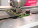
4. Placement: The placement of μBGAs and LGAs in the rework process requires the simultaneous viewing of pads and leads at an adequately high magnification (i.e., 30-50X). Once the images of the pads and leads have been aligned, the component is placed onto the board.
For most LGAs, viewing at 25X magnification should be sufficient; however, 50X magnification is required with BGAs because of the smaller size of these packages to ensure that the balls and pads are properly registered and aligned.
5. Reflow: As previously mentioned, it is critical to apply a uniform, repeatable reflow profile. Profile setup is the key to successful reflow, and the proper placement of thermocouples during testing ensures uniform temperature across the component and the PCB assembly.
Process control
The rework equipment must provide all the necessary functions described in the rework process above. The level of process control is especially critical in the reflow procedure, whether in the removal or replacement mode; although improper site cleaning, solder paste deposition and component placement can be corrected by repeating the process. Poor process control in reflow can destroy the component, the board or adjacent components.
The equipment should offer the appropriate balance between the level of process control provided and the ease and simplicity of equipment operation. A graphical interface enables the operator to visualise the temperature parameters during rework and save the actual process graph for verification and future analysis. Additionally, it is important that operators and technicians be properly trained and have the equipment available to properly identify any defective components.
Conclusion
All the factors that make the μBGA package more attractive than peripheral-leaded devices in the assembly environment carry through to rework. For example, the ease of solder or flux deposition on a µBGA pad pattern and the ease of alignment and placement of µBGAs with image overlay technology makes µBGA rework easier in comparison to fine-pitch QFPs.
With the introduction of high-quality, lower-priced convection array rework systems, users have the benefits of an easy-to-use system combined with the technology and process control to ensure repeatable results.
For more information contact Test & Rework Solutions, +27 (0)11 704 6677, [email protected], www.testandrework.co.za
| Tel: | +27 11 704 6677 |
| Email: | [email protected] |
| www: | www.testandrework.co.za |
| Articles: | More information and articles about Test & Rework Solutions |


© Technews Publishing (Pty) Ltd | All Rights Reserved
 printer friendly version