


The low inductive strip line concept offers several benefits regarding the switching behaviour of IGBT modules, but for implementation in real packages a lot of boundary conditions have to be considered. This article describes a possible implementation of a low inductive strip line concept for symmetric switching in a new high-power module.
The influence of a low inductive and symmetric concept on clean switching has already been shown in several publications – see References section. The design of the internal conductors, the arrangement of the chips and the connection of the internal conductors, either to the insulation ceramics or to the external bus bar system, contribute strongly to the stray inductance and to the symmetry of the module.
The best concept for a low inductive design is the use of half bridge IGBT modules. They offer the possibility to keep the commutation path between the upper and lower switch very short by implementing both switches on insulated ceramics with only internal, low inductive connections.
Strip line design
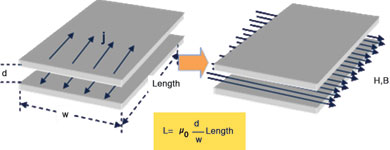
The internal conductors from the external DC terminals to the IGBTs and diodes are preferably designed as strip lines. The inductance of two strip line conductors carries the same current in opposite directions, as shown in Figure 1.
From the formula in Figure 1 it seems to be very easy to generate a low inductance design: keep the connectors short, make them very wide and reduce their separation as much as possible. But there are some constraints to be considered.
IGBT module size determines design layout
The stray inductance is mainly a function of the dimensions of the conductor sheets used, so the outside dimensions of the module mainly determine the design of these parts. For ideal switching behaviour it is favourable to arrange all chips in a single row. In this case the number of chips defines the width of the module. But in reality this would lead to a very long, narrow construction that will not fit all requirements for a minimised system size. Therefore the width of the internal strip line is limited by the size of the paralleled dies.
For this study a chip layout was chosen, where a nominal current of 700 A for the upper and lower system can be implemented. The width of the module is approximately 80 mm. Taking into account that additional space is needed for the housing and clearance for assembly, the maximum possible usable width is smaller than the module width.
Especially with higher blocking voltages, e.g. 3300 V and above, the IGBT package has to fulfil the standards for clearance and creepage distances. Within IEC 60664-1 the required distances for insulation coordination are described.
Minimum distances depend on the voltage classification and the housing material. A way to fulfil the creepage distances and minimise the clearance between the terminals is the implementation of grooves and a housing material with a high CTI. In this example a minimum required creepage distance of 28 mm leads to spacing between the terminals of 14 mm.
In this study we consider feeding the DC current into the middle of the IGBT module. Driver mounting directly on the module offers the possibility for a low inductive connection to the driver.
For half bridges with auxiliary collector contacts there are three different voltage levels on the driver board that require certain spacing. To maximise the area for a driver board, it is favourable to move the DC terminals to the edge of the power module and utilise the space in the middle. Unfortunately this will increase the length of the internal conductor. A possible solution is a sloped design whereby the length of the conductors can be reduced compared to a solution with perpendicular bends.
Distance between the conductors
To separate the potential between DC+ and DC– conductors, an insulation layer is needed in between. In order to achieve a low inductance, the thickness of this material has to be kept thin. One possibility is the use of very thin heat resistant foils. With Polyimide or Teflon foils a thickness of 0,2 mm and less could be possible on the basis of the insulation stability.
The difficulty with using foils is the manual assembly required and the need to keep it safely in place. This is possible with insertion into an injection mould and embedding the conductors with plastic. The disadvantage is this is a costly process and delamination is possible in thermal cycling conditions.
With conventional injection moulded spacers a typical thickness of the plastic material without having the risk of pin holes or other defects is ~1 mm. In the overall design the effect of the thickness of the insulation layer was calculated in simulations of different variants. The result is shown in Figure 2.
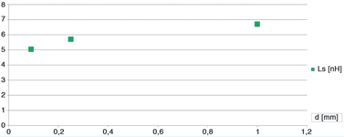
For a 0,1 mm foil the inductance could be as low as 5 nH. Based on the above described boundary conditions, the use of a plastic spacer is preferred and leads to a stray inductance of approximately 7 nH.
Connection to the chip
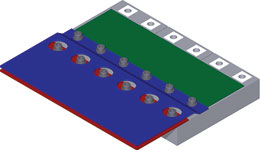
If we take a closer look at the connection of the conductors to the ceramic substrates, unfortunately there is no way to connect in a ‘line’. With a placement of the leads in between high-side and low-side IGBTs there has to be a separate potential for the commutating current. In Figure 3 possible points for connections are shown.
Instead of using one single point, several connections as wide as possible were made. Figure 3 shows the IGBTs and diodes of the upper switch on the left side, and the lower switch on the right side. The red areas show the connections to the DC+ conductor, while the blue areas show the position of the DC– potential. The white arrows describe the area where the commutation current is flowing. The green areas show possible positions of the AC terminal.
Connection to the external bus bar system
Another important interface of the IGBT module is the connection to the DC bus bar. The bus bar itself is an ideal strip line concept with wide conducting plates and a thin insulation sheet.
This concept has to be sacrificed at the connection points, especially when screw terminals are used. These short interruptions of the strip line have a big impact on the overall outcome. For low- and medium-power devices the connection to the DC link can be realised with press fit pins and a PCB with reinforced copper layers. Paralleling with multiple connection points reduces inductance in this area.
In high-current and high-voltage applications the contacting of the IGBT module to an external bus bar system is usually realised with screw connections. The bus bar system is made of laminated metal sheets of copper or aluminium. To realise a reliable connection with little losses, screws are the most common connectors. They offer high contact forces that reduce contact resistance; furthermore, they are easily available and can be assembled with standard equipment
Conclusion
Even for high-power modules with high blocking voltages and high output currents, a low inductive design using the strip line concept is possible. Legal regulations and standards create several constraints that do not allow the implementation of an ideal solution. Nevertheless, an IGBT study with a stray inductance of approximately 7 nH at a nominal current of 700 A was realised. For future applications this will enable the use of fast switching devices. With reduced switching losses higher switching frequencies could be implemented.
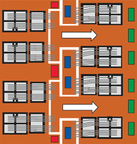
The concept also allows an easy way to connect several IGBT modules in parallel with the use of one common DC bus bar (Figure 4). In a three-module parallel configuration this will lead to 2 nH for a configuration with a nominal output current of 2100 A per system.
References
[1] R. Bayerer, D. Domes: Power circuit design for clean switching, CIPS, 2010.
[2] R. Bayerer, D. Domes: Power circuit design for clean switching, ECPE, 2011.
For more information contact Davis Moodley, Infineon Technologies, +27 (0)11 706 6099, www.infineon.com


© Technews Publishing (Pty) Ltd | All Rights Reserved
 printer friendly version