Void-free reflow soldering technology
23 October 2013
Manufacturing / Production Technology, Hardware & Services
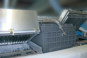
SEHO Systems has developed a new technology for virtually void-free soldering results with the MaxiReflow HP.
Whether for power electronics, electronic aviation systems, medical equipment or electronic systems for the automotive industry, voids in solder joints represent one of the main problems. Enclosed voids can cause a displacement of electrical and thermal paths as well as a local concentration of power and heat. Additionally, gas voids are quick to form spheres in the solder gap, which could cause the tilting of chip components and a wedge-shaped solder gap.
The amount of voids can be influenced by different measures such as good wettability of metallisation, solder pastes with special adopted solvents and an adequate preheating profile. However, to achieve virtually void-free solder joints, a special vacuum process step during soldering was demanded.
This vacuum process is associated with some essential disadvantages. Apart from the technical expenses for vacuum pumps and additional locks, the vacuum process excludes the use of gas convection for heating, resulting in an uneven heat distribution on the assemblies.
SEHO’s MaxiReflow HP now offers innovative technology that combines convection heat and a special hyper-pneumatic module, thus ensuring virtually void-free solder connections. Instead of using a complicated vacuum process, the system is equipped with an effective excess pressure chamber, allowing shorter cycle times and enabling gas convection to be used for heating assemblies.
Each heating zone of the MaxiReflow HP – as well as the zones integrated in the hyper-pneumatic chamber – has a tangential fan that ensures absolutely homogeneous heat distribution with the large volume of ventilated process gas. This enables the most effective and component-sensitive heating of the products with set temperatures on a low level.
When processing uncritical assemblies, the MaxiReflow HP can also be operated without activating the hyper-pneumatic chamber. In this case, the printed circuit boards go through a conventional reflow soldering process.
For more information contact Igmar Grewar, Quamba Technologies, +27 (0)83 417 4294, [email protected], www.quamba.co.za
Further reading:
FineX: Makes shielding clear
Avnet Abacus
Manufacturing / Production Technology, Hardware & Services
Panasonic Industry launches high-transparency, low-resistance, flexible transparent conductive film for electromagnetic wave shield with pre-applied OCA.
Read more...
Collaboration is now critical
RS South Africa
Manufacturing / Production Technology, Hardware & Services
The message emerging from RS Connect is clear: Organisations can no longer rely on internal optimisation alone to secure performance. Competitive advantage is increasingly being determined by the strength of external relationships, shared capability and coordinated action across value chains.
Read more...
Disruption is the new normal. Effortless is the new competitive advantage.
Seven Labs Technology
Manufacturing / Production Technology, Hardware & Services
Global supply chains have been under pressure for years. The manufacturers still standing are the ones who stopped waiting for normal to return, and started building something better.
Read more...
World-first 016008 mm component placement
Manufacturing / Production Technology, Hardware & Services
Fuji has achieved the world’s first placement of 016008 mm (0,16 x 0,08 mm or 006 x 003 inches) size components on printed circuit boards with its SMT pick and place machine, NXTR.
Read more...
Lifecycle and obsolescence: Protecting electronics through process
Production Logix
Manufacturing / Production Technology, Hardware & Services
At Production Logix, we believe longevity is not accidental. It is engineered through early visibility, structured response, and disciplined execution, in partnership with our OEM customers.
Read more...
Maximising squeegee quality and durability
Testerion
Manufacturing / Production Technology, Hardware & Services
Transition Automation has announced two new product advancements designed to improve SMT printing performance and extend squeegee life: laser-enhanced Permalex bonding and integrated edge protectors.
Read more...
NeoDen ND2 PCB screen printer
ZETECH ONE
Manufacturing / Production Technology, Hardware & Services
The NeoDen ND2 PCB screen printing machine is a fully automatic stencil printer designed to deliver precise and consistent solder paste application in modern SMT production environments.
Read more...
Understanding the BGA rework process
Techmet
Manufacturing / Production Technology, Hardware & Services
BGA rework is a highly technical process that involves removing the faulty component, preparing the circuit board, and installing a new or repaired device, while maintaining the integrity of the printed circuit board.
Read more...
Flexible three-process reflow soldering system
Truth Electronic Manufacturing
Manufacturing / Production Technology, Hardware & Services
By combining multiple soldering technologies within a single system, the Vision TripleX system enables manufacturers to adapt easily to different assembly requirements, board designs, and production volumes.
Read more...
Inline vapour phase soldering for high-volume production
MyKay Tronics
Manufacturing / Production Technology, Hardware & Services
The VP2200-100 vacuum inline vapour phase soldering system from ASSCON is designed for fully automated, high-volume electronics manufacturing where process consistency and solder joint quality are critical.
Read more...


 printer friendly version