16 July 2014Manufacturing / Production Technology, Hardware & Services
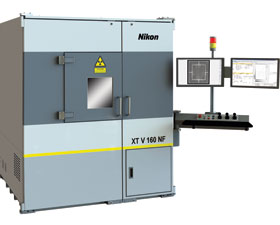
Nikon Metrology’s latest XT V 160 NF is a high-precision, flat-panel based X-ray inspection system that facilitates real-time imaging and defect analysis of next-generation wafer-level, semiconductor device and PCBA (printed circuit board assembly) applications.
The system’s NanoFocus source with nanoscale X-ray spot size, high-precision manipulator and 3 megapixel flat panel detector with high dynamic range results in feature recognition capability below 0,1 μm. The large 580 x 580 mm tray enables the possibility to inspect large PCBAs, multiple components or pallets, coupled with advanced automated software capabilities.
The machine features a 360° continuous rotate detector axis which enables oblique angle views of up to 60° to the centre of the detector panel. The system offers intelligent region-of-interest lock, which maintains feature view with changing magnification or angle view.
Thanks to the highly accurate and precise anti-vibration sample manipulator, the NF system is ready for next-generation laminography inspection techniques with advanced cross sectional view capability to detect defects as small as a few microns. It provides a method of inspecting a region of interest which can be challenging to inspect with 2D radiography, such as 3D stack dies, BGA pad cracks or multilayer boards, without the need to rotate the sample or cut it down in size.
The system is equipped with Inspect-X 4 acquisition and analysis software focusing on improved usability and productivity. The software facilitates real-time inspection as well as the creation of automated programs via a user-friendly graphical user interface.
Productivity is increased by offering intuitive operator control, fast creation of inspection programs and robust image inspection algorithms. The new range of intelligent inspection tools features enhanced image processing offering advanced BGA and wire sweep analysis to analyse the most challenging electronics boards and components
World-first 016008 mm component placement
Manufacturing / Production Technology, Hardware & Services
Fuji has achieved the world’s first placement of 016008 mm (0,16 x 0,08 mm or 006 x 003 inches) size components on printed circuit boards with its SMT pick and place machine, NXTR.
Read more...Lifecycle and obsolescence: Protecting electronics through process Production Logix
Manufacturing / Production Technology, Hardware & Services
At Production Logix, we believe longevity is not accidental. It is engineered through early visibility, structured response, and disciplined execution, in partnership with our OEM customers.
Read more...Maximising squeegee quality and durability Testerion
Manufacturing / Production Technology, Hardware & Services
Transition Automation has announced two new product advancements designed to improve SMT printing performance and extend squeegee life: laser-enhanced Permalex bonding and integrated edge protectors.
Read more...NeoDen ND2 PCB screen printer ZETECH ONE
Manufacturing / Production Technology, Hardware & Services
The NeoDen ND2 PCB screen printing machine is a fully automatic stencil printer designed to deliver precise and consistent solder paste application in modern SMT production environments.
Read more...Understanding the BGA rework process Techmet
Manufacturing / Production Technology, Hardware & Services
BGA rework is a highly technical process that involves removing the faulty component, preparing the circuit board, and installing a new or repaired device, while maintaining the integrity of the printed circuit board.
Read more...Flexible three-process reflow soldering system Truth Electronic Manufacturing
Manufacturing / Production Technology, Hardware & Services
By combining multiple soldering technologies within a single system, the Vision TripleX system enables manufacturers to adapt easily to different assembly requirements, board designs, and production volumes.
Read more...Inline vapour phase soldering for high-volume production MyKay Tronics
Manufacturing / Production Technology, Hardware & Services
The VP2200-100 vacuum inline vapour phase soldering system from ASSCON is designed for fully automated, high-volume electronics manufacturing where process consistency and solder joint quality are critical.
Read more...Global electronics solutions since 1964 IMP Electronics Solutions
Manufacturing / Production Technology, Hardware & Services
Over more than six decades, IMP Electronics Solutions has built a reputation for technical expertise, reliable supply chains, and strong partnerships with both customers and manufacturing partners.
Read more...Driving excellence in electronics manufacturing Jemstech
Editor's Choice Manufacturing / Production Technology, Hardware & Services
Jemstech’s reputation for disciplined execution and client-focused service has earned it strong loyalty from companies operating in demanding industries.
Read more...When do you need Nitrogen in reflow? Truth Electronic Manufacturing
Manufacturing / Production Technology, Hardware & Services
Nitrogen in reflow soldering is often seen as a performance enhancer, offering improved wetting, shinier joints, and fewer defects. But it is not always necessary.
While every effort has been made to ensure the accuracy of the information contained herein, the publisher and its agents cannot be held responsible for any errors contained, or any loss incurred as a result. Articles published do not necessarily reflect the views of the publishers. The editor reserves the right to alter or cut copy. Articles submitted are deemed to have been cleared for publication. Advertisements and company contact details are published as provided by the advertiser. Technews Publishing (Pty) Ltd cannot be held responsible for the accuracy or veracity of supplied material.


 printer friendly version