


Despite the wide variety of applications, certain panel sizes have proven to be particularly viable in the manufacturing process of electronic assemblies.
On the one hand, this is due to the capacities for handling the panels inside the production machines, such as solder paste printers, pick-and-place machines, ovens, AOI and magazine stations. On the other hand, ergonomics plays an important role when the panels are handled by operating personnel, as well as the weight of the assemblies.
The dimensions of the panels depend primarily on the respective application. As a rule, the edge lengths of individual assemblies are less than half a metre. Assemblies that are significantly smaller are generally produced on a multiplier. This results in increased throughput and optimal utilisation of the machines in production. However, larger assemblies are more problematic. Most standard systems can no longer process these oversized assemblies.
What is the reason for large printed circuit boards?
Despite the trend towards miniaturisation and integration in electronics, applications with particularly large individual assemblies continue to arise. Lighting technology is one example: current developments in LED technology can now be found in all types of lighting, with increased luminous fluxes, generation of different colours, improved efficiency and production in a wide range of shapes.
In contrast to other electronic assemblies, size is often more important than miniaturisation where the production of lights is concerned. There are significant advantages when a larger LED light is produced on a single carrier, rather than assembling it from individual components. These include the elimination of expensive and error-prone connectors and cables, a reduction in the installation and service effort required, the integration of heat management, as well as an increase in the service life of the product.
An automatic optical inspection (AOI) system is indispensable for the efficient and automated production of assemblies. It is primarily used for quality assurance, but also for the quick and reproducible detection of production faults. In addition to standard tests for the presence of components and an assessment of solder joints, these can also include distance and position measurements (e.g. the distance of a QFN to a register mark), a swash circumference test of connector pins, or to take a more exotic example, the alignment of reed contacts in their glass bodies. AOI and automatic contacting even make it possible to extend the test of a lighting assembly to include the functional testing of LEDs, detection of micro cracks in the LED bodies, or even brightness and radiation measurements.
AOI is also an important element for achieving complete traceability of assemblies, as well as for the immediate statistical evaluation of the errors and measured values determined. The large amount of data collected is structured according to any specifications required and exchanged with a production control system (MES interface). This system can then intervene immediately in the upstream production, based on the information obtained.
If a manufacturer is tasked with the production of an extra-long assembly, this may mean that series production using an automated line is impossible, and production steps must be carried out manually. Alternatively, an assembly line with special machinery can be set up exclusively for these products. The latter option is usually considerably more expensive, making it barely profitable for small and medium-sized series production. Ideally, production machines can be set up for this special task using simple retooling measures.
There are a large number of AOI system providers worldwide. Most of the manufacturers naturally focus on the standard, widely used applications in order to achieve high sales volumes and low machine prices. The European industry, however, is increasingly characterised by its ability to flexibly and quickly react to special requirements with low and medium quantities, instead of providing for the cheap mass production of a single product. This applies for consumer goods as well as industrial equipment.
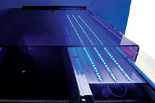
So how can a conventional inline AOI, which is designed for standard assemblies and panels, be equipped for long-board inspection? Section-by-section inspection is one option. To do so, the standard AOI is extended on both sides by two belt modules of equal length, to ensure the smooth forward feed of the long assembly. During operation, this is then transported forward, fixed and tested inside the AOI several times at defined intervals. The data and test results for each test section are grouped together and form the overall result for the assembly.
An X-Y axis gantry is used to position the image acquisition system in relation to the assembly. The assembly must be stationary while doing so. To ensure a complete inspection, the forward feed between the test sections should be slightly smaller than the possible test area in the transport direction of the AOI.
The number of the sections to be tested for the overall inspection is based on the length of the assembly, divided in whole numbers by the length of the forward feed. This method means that the maximum length of an assembly to be tested is only limited by the selection of the belt modules attached.

Göpel Electronic offers this concept as a modular extension to the AOI systems. The belt modules are supplied separately and are only connected to the AOI on-site. The electrical interface is established easily and quickly via connectors for power supply and network. A system of several stoppers ensures that the forward feed between the test section is defined and takes place quickly. The assembly is fixed in the test area. Despite this, protruding sections are supported and the assembly is not exposed to bending. This also makes it possible to test flex PCBs using a corresponding carrier.
It is equally easy to create a test programme. The individual test sections are generated from the CAD data of the assembly and associated with test tasks. The program parts of the sections are then combined into a so-called multi-test and are processed sequentially. It also remains possible to work with changing product versions and to carry out tests on standard-length assemblies. The image acquisition concept, with its telecentric optics, orthogonal camera, 3D images without shading and freely selectable angled views, is just as universally applicable and equal to any test situation.
This concept is part of the overall modular and flexible design of optical inspection systems by Göpel Electronic, which can be tailored to client requirements depending on speed, test depth and budget.
| Tel: | +27 11 869 0049 |
| Email: | [email protected] |
| www: | www.mykaytronics.co.za |
| Articles: | More information and articles about MyKay Tronics |


© Technews Publishing (Pty) Ltd | All Rights Reserved
 printer friendly version