


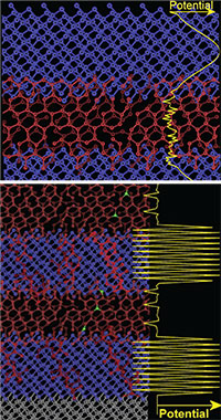
Through their work, the group reported one of the first theoretical models that can explain the fundamental electronic transport properties in disordered carbon superlattices.
Superlattices are made up of alternating layers of very thin semiconductors, just a few nanometres thick. The layers are so thin that the physics of these devices is governed by quantum mechanics, where electrons behave like waves. In a paradigm shift from conventional electronic devices, exploiting the quantum properties of superlattices holds the promise of developing new technologies.
The group, headed by Professor Somnath Bhattacharyya, has been working for the past 10 years on developing carbon-based nano-electronic devices. “Carbon is the future in the electronics field and it soon will be challenging many other semiconductors, including silicon,” he stated.
Bhattacharyya started looking at the use of carbon for semiconductor applications almost 10 years ago, before he joined Wits University, when he and co-authors from the University of Surrey developed and demonstrated negative differential resistance and excellent high-frequency properties of a quantum device made up of amorphous carbon layers. This work was published in Nature Materials in 2006.
The physics of carbon superlattices is more complex than that of crystalline superlattices (such as gallium arsenide), since the material is amorphous and carbon atoms tend to form chains and networks. The Wits group, in association with researchers at the University of Surrey in the UK, has developed a detailed theoretical approach to understand the experimental data obtained from carbon devices. The paper was published in Scientific Reports (Nature Publishing Group) last October.
“This work provides an understanding of the fundamental quantum properties of carbon superlattices, which we can now use to design quantum devices for specific applications,” said lead author, Wits PhD student Ross McIntosh. “Our work provides strong impetus for future studies of the high-frequency electronic and optoelectronic properties of carbon superlattices.”
McIntosh undertook the opportunity at honours level to measure the electrical properties of carbon superlattice devices. Now, as a PhD student and having worked extensively with theoretician Dr. Mikhail V. Katkov, he has extended the theoretical framework and developed a technique to calculate the transport properties of these devices.
Bhattacharyya believes this work will have immense importance in developing carbon-based high-frequency devices. “It will open not only fundamental studies in carbon materials, but it will also have industrial applications in the electronic and optoelectronic device sector,” he believes.
Superlattices are currently used as state of the art high-frequency oscillators and amplifiers, and are beginning to find use in optoelectronics as detectors and emitters in the terahertz regime. While the high-frequency electrical and optoelectronic properties of conventional semiconductors are limited by the dopants used to modify their electronic properties, the properties of superlattices can be tuned over a much wider range to create devices which operate in regimes where conventional devices cannot.
Superlattice electronic devices can operate at higher frequencies and optoelectronic devices can operate at lower frequencies than their conventional counterparts. The lack of terahertz emitters and detectors has resulted in a gap in that region of the electromagnetic spectrum (known as the ‘terahertz gap’), which is a significant limitation, as many biological molecules are active in this regime. This also limits terahertz radio astronomy.
Amorphous carbon devices are extremely strong, can operate at high voltages and can be developed in most laboratories in the world, without sophisticated nano-fabrication facilities. New carbon-based devices could find application in biology, space technology, science infrastructure such as the Square
Kilometre Array (SKA) telescope in South Africa, and new microwave detectors.
“What was lacking earlier was an understanding of device modelling,” explains Bhattacharyya. “If we have a model, we can improve the device quality, and that is what we now have.”
About the Wits Nanoscale Transport Physics Laboratory
The Wits Nanoscale Transport Physics Laboratory (NSTPL) was established in 2009 under the leadership of Professor Somnath Bhattacharyya when Professor João Rodrigues was the head of the School of Physics at the University of the Witwatersrand, South Africa. The department is known as a leading physics school on the African continent, having one of the largest academic staff complements on a single campus.
Since the opening of the laboratory, the NSTPL has gone from strength to strength in establishing a facility that houses world class fabrication and measurement equipment, an initiative strongly supported by research entities such as the NRF, CSIR, Wits Research Office and DST/NRF Centre of Excellence in Strong Materials.
The NSTPL is well equipped with various sophisticated synthesis facilities, as well as a cryogenic micro-manipulated probe station to conduct sensitive quantum transport measurements at temperatures near absolute zero. The NSTPL also houses a fully operational electron beam lithography scanning electron microscope, used to fabricate nanoscale devices based on these carbon materials.
Some noteworthy current projects include the fabrication of spintronic devices using supramolecular Gd-functionalised carbon nanotubes, the fabrication of graphene field effect transistors, and most recently the study of the unconventional superconductivity observed in boron-doped diamond. The NSTPL group has also published a number of papers on theoretical investigations, led by Dr Mikhail Katkov and Dr Dmitry Churochkin, on the role of disorder on the quantum transport in carbon systems. These various topics form part of the broader direction the group has taken, that being to investigate the physics of carbon materials in the hopes of finding application in quantum information systems as well as detector devices valuable for space exploration.
For more information contact Schalk Mouton, Wits University, +27 (0)11 717 1017, [email protected]


© Technews Publishing (Pty) Ltd | All Rights Reserved
 printer friendly version