


Part I of this paper discussed data acquisition as applied to a loadcell sensor and briefly intriduced three tyes of noise - device noise; conducted noise; and radiated noise. We now take an in-depth look at the first of these: device noise
Device noise can be classified into two groupings, passive and active. Passive devices are constructed with materials, such as films and composites. Components such as resistors, capacitors, inductors, transformers, and conductors fall into this category. Active devices are fabricated in silicon. This class of device includes bipolar transistors, field effect transistors, CMOS transistors and integrated circuits that use these transistors.
When device noise issues are described, the terminology and units of measure are somewhat different than the engineering language that is used to describe voltage, current and number of bits. The fundamental differentiation is that noise signals are by definition uncorrelated. As a consequence the simple addition of voltage or current noise sources or regions are implemented with the formula 'the square root of the sum of the squares' or:
V2 total = V12 + V22 + ... + VN2
or
I2 total = I12 + I22 + ... + IN2
This formula applies to noise contributions over a specific bandwidth (BW). BW is defined as the equivalent noise bandwidth. If a bandwidth is not defined, a particular frequency must be. In this case, the noise units are V/sHz or A/sHz. These units of measure describe the voltage or current noise density (also known as spot noise). This noise is measured at a specific frequency over a 1Hz bandwidth. If the noise density across a frequency region is consistent, that noise density can be multiplied by the s(BW) to convert the noise density to noise.
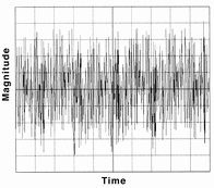
Peak-to-peak noise can be a calculated value or an assessment of minimums and maximums over a large sample size. A scope photo of noise over time is shown in Figure 3. Visually it can be seen that the peak-to-peak noise of this sample is approximately eight divisions on the y-axis.
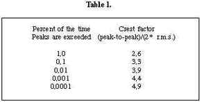
The peak-to-peak calculation predicts the probability that over time each occurrence of the signal in question will fall within a specified range. In the calculation, the RMS value of a large sample is defined as one standard deviation of the resultant gaussian distribution. The RMS (one standard deviation) noise can then be multiplied by a constant to convert that RMS number to a peak-to-peak estimate. The constant that is used is called a crest factor (see Table 1).
For instance, if 4096 output samples are taken from a system that has a DC input excitation, the RMS output noise is equal to one standard deviation of the 4096 samples. If this RMS value is equal to 1 µV r.m.s., an estimate of peak-to-peak performance of the system can be calculated by multiplying the RMS value times 2*crest factor. A crest factor of 3,3 can be used to calculate a peak-to-peak output noise estimate of 6,6 µVp-p with a 0,1% probability that future samples will exceed ±3,3 µV centred around the average expected output. Calculated peak-to-peak noise is typically more conservative.
Passive devices
Resistors: There are three basic classes of fixed resistors:
* Wirewound.
* Film type.
* Composition.
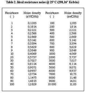
Regardless of their construction, all resistors generate a noise voltage. This noise is primarily a result of thermal noise. The lower quality resistors, such as the composition type, have additional noise in the lower frequency spectrum due to shot and contact noise. Thermal noise, which is also called Johnson noise, is generated by the random thermal motion of electrons in the resistive material and can never be lower than ideal. It is independent of DC current flow and is constant across the entire frequency spectrum.
The ideal thermal or Johnson noise for resistors is:
VN = s(4KTR(BW)).
where K is equal to Boltzman's constant which is 1.38e-19.
T is equal to temperature in Kelvin.
R is the resistance value in ohms.
(BW) is the noise bandwidth of interest.
The ideal calculated noise of various values of resistance is shown in Table 2.
Wirewound resistors are the quietest of the three and come close to ideal noise levels. Composition resistors are the noisiest because of their contact noise, which is aggravated by current. Otherwise composition resistors have the same noise as wirewound.
Spice simulations can be used to perform 'what ifs' with device noise problems such as resistor noise. The total noise contribution of the instrumentation amplifier structure in Figure 1 from DC to 10 MHz is 814 µV r.m.s. and 677 µV r.m.s. from DC to 100 kHz. If the resistors in this circuit are increased by 10x the total noise contribution of this circuit is 930 µV r.m.s. out to 10 MHz and 728 µV r.m.s. out to 100 kHz. If the resistors are reduced by 10x, the total noise contribution is 787 µV r.m.s. to 10 MHz and 671 µV r.m.s. out to 100 kHz. If a low pass anti-aliasing filter is not used in this circuit, the noise contribution due to the resistors in Figure 1 is significant.
Capacitors: In noise discussions, capacitors are generally identified as the device that reduces or filters system noise. Capacitors are most frequently categorised by the dielectric material that they are made of. Each type of capacitor has characteristics that make them suitable for certain applications.
For instance, the large capacitance values of electrolytic capacitors in a small case offer a distinct advantage in terms of board layout. They are most often used for low frequency filtering, bypassing and coupling. As a disadvantage, electrolytic capacitors are polarised and a DC voltage must be maintained across them. In contrast, the series resistance of paper and mylar capacitors is considerably less than electrolytic capacitors. These capacitors are medium frequency devices and useful up to a few megahertz. Paper and mylar capacitors are typically used for filtering, bypassing, coupling, timing and noise suppression. Mica and ceramic capacitors have very low series resistance and inductance. These are high frequency devices that are useful up to about 500 MHz if the leads are kept short. These capacitors are usually used for high-frequency filtering, bypassing, coupling, timing and frequency discrimination. They are also very stable with respect to time, temperature and voltage. Polystyrene capacitors have extremely low series resistance and very stable capacitance-frequency characteristics. These devices are the closest to the ideal capacitor. Typical applications include filtering, bypassing, couple, timing and noise suppression.
Inductors and transformers: An ideal inductor would only have inductance, but actual inductors also have series resistance and distributed parallel capacitance between windings. An important characteristic is their susceptibility to and generation of stray magnetic fields. Two inductors that are intentionally coupled form a transformer. Transformers are usually used to provide isolation between two circuits, by breaking ground loops or signal paths or power generation. These devices are typically noise generators because of the switching activity associated with isolation.
Active devices
Pure analog devices - This category of devices include operational amplifiers, instrumentation amplifiers, voltage references, voltage regulators, to name a few. These devices are typically specified in terms of nV/sHz, pA/sHz, µV r.m.s. or µVp-p. The noise that is generated by these devices can be defined as current noise or voltage noise, both of which have two fundamental regions. The two fundamental regions of noise that these devices produce are the 1/f and broadband regions.
1/f noise is also known as contact noise or flicker noise. This is low frequency noise where the power density varies as the reciprocal of frequency (1/f). This noise is a consequence of trapped carriers in the semiconductor material, which are captured and released in a random manner. The time constant of this energy is concentrated within lower frequencies. 1/f noise is shown graphically in Figure 4.
Shot noise on the other hand is associated with the DC current flow across a p-n junction. This noise is due to random diffusion of carriers through the base of the transistor and random generation and recombination of hole electron pairs.
The RMS noise current is equal to ISH = s2qIDC (BW), where q is electron charge (1.6e-19 coulombs), IDC is the average DC current in amperes and (BW) is the noise bandwidth in Hertz. The noise contribution from this source is generally seen in the higher frequencies or the broadband area shown in Figure 4.
Part III will follow in a subsequent issue of Dataweek and will look at conducted noise in embedded systems. For further information contact Willem Hijbeeck, Tempe Technologies, (011) 452 0530.
| Email: | [email protected] |
| www: | |
| Articles: | More information and articles about Tempe Technologies |


© Technews Publishing (Pty) Ltd | All Rights Reserved
 printer friendly version