


The effective removal of heat from electronic systems has long been a topic that is high on the agenda of engineering professionals – especially those tasked with shrinking designs from a size and weight perspective, while also adding extra functionality. As space for deploying cooling mechanisms reduces and power levels simultaneously increase, the challenge becomes ever greater.

Experienced engineers will say that the best way to deal with heat is to not generate it in the first place. While theoretically speaking that is a valid point, in reality it is difficult to accomplish (despite the best endeavours of semiconductor manufacturers to raise power efficiency benchmarks). The next best approach is to ensure that any excess heat is carried away as quickly and effectively as possible from its source to the ambient air.
This article will step beyond the realm of traditional thermal management solutions (such as fans, blowers and heatsinks) and look at the way that the latest IC packaging technologies are making a significant contribution to satisfying the exacting thermal demands of modern electronic designs.
Semiconductors come in all shapes and sizes, covering a broad range of product types – from complex microcontroller units through to simple, single-function, discrete devices. The discrete devices, such as MOSFETs and IGBTs, used in power applications are a key focus for thermal improvement as they have the potential to generate significant quantities of heat energy if not optimised.
Semiconductor manufacturers have gone to great lengths to improve on-state resistance (RDS(ON)), thereby mitigating the static losses of these devices, as well as reducing important output parameters, such as COSS, which impact on switching losses. Alongside improvements to semiconductor processes, advances in component packaging are also responsible for enhancing the thermal performance.
Replacing wire bonds
One of the most popular packages for MOSFET devices is the DPAK. This small (6,5 x 9,5 x 2,3 mm) surface-mount device incorporates a metal tab for thermal conduction and mechanical strength. The small size and ability to be auto-placed have made it very appealing, although in the most space-constrained applications, many components used are now of a lower profile.
Another drawback of the DPAK arrangement is that the semiconductor die is connected to the leadframe via wire bonds. These 70 μm bonds limit the current handling capability of the device and create a not insignificant resistance path which leads to sizeable amounts of heat being generated.
To overcome these problems, ON Semiconductor recently announced the ATPAK next-generation package for discrete power devices such as MOSFETs. The ATPAK maintains exactly the same footprint as the DPAK, but reduces the height from 2,3 mm to just 1,5 mm, making it highly suitable for new ultra-thin applications as well as for retrofitting to upgrade existing designs. A unique copper clip structure is used which replaces the thin wire bonds found in DPAK devices, and boosts both the thermal and electrical capabilities as a result.
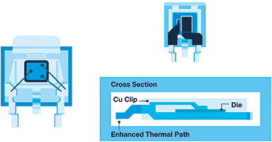
As the clip has a much larger cross-sectional area, the RDS(ON) figure is substantially lowered, with static losses consequently being a lot less. I²R losses are also kept in check, thus curbing heat generation in the device. The strong thermal conduction capabilities of the copper clip are far better than those of conventional wire bonds, so heat generated from the semiconductor junction is rapidly transferred to the package pins, allowing it to be dissipated into the PCB. As an additional benefit the clip’s greater cross-sectional area and reduced resistance also allows heightened current handling.
Testing against a standard DPAK device under identical conditions has seen the ATPAK exhibit case and junction temperatures of 74,8°C and 76,0°C respectively when set with dissipating 1,44 W. By comparison the DPAK’s figures were 80°C and 82,2°C. This translated into ATPAK offering greater long-term device reliability as well as requiring significantly less cooling, despite the 35% reduction in volume when compared to DPAK.
Top-side cooling allows SMD device use in challenging power applications
In high-power application settings it is still relatively common to use through-hole switching MOSFET devices in popular packages, such as TO-220 or TO-247, as they often simplify the task of cooling the design. Since these packages can be fixed directly to heatsinks, they generally provide a more closely-coupled thermal path than SMD devices that most often dissipate heat through the PCB.
However, there are a couple of issues with this approach. The longer leads of conventional packages have relatively large parasitic inductances associated with them, which prevents efficient high-speed switching topologies from being used. Also, as pin-through devices require a different placement and soldering process, they add both cost and complexity to manufacturing of the end product.
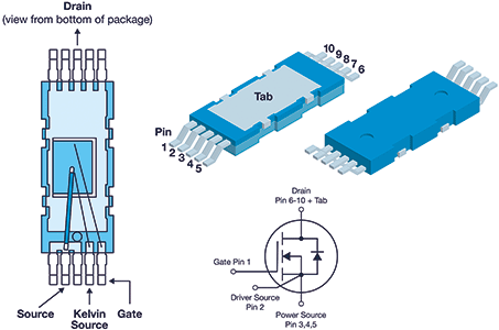
While conventional SMD packages rely on dispersing heat through the PCB, the new DDPAK package from Infineon Technologies is a surface-mountable package format for power devices with top-side cooling via a heatsink, thereby benefitting from the natural rising of heat. The packaging concept is optimised for high-power, high-voltage and high-reliability applications and is suitable for MOSFETs and SiC diodes alike – both of which are essential to modern power designs.
Although DDPAK and the associated semiconductor technologies, such as Infineon’s CoolMOS G7 or CoolSIC G6, are very thermally efficient, for almost all practical applications some form of heatsinking will still be required – attached to the top-side of the device.
The package design provides several options for affixing the heatsink, including the use of clips, thermally conductive adhesives or direct soldering. The surface is compatible with the application of gap fillers or gap pads to ensure that the highest levels of thermal conductivity are derived. DDPAK packages offer five connections for the drain current, three source connections and a source sense connection.
This multi-pin approach is not possible with standard TO-220 or TO-247 packages and provides cleaner waveforms that reduce losses, and therefore combats heat generation. This format is smaller than a TO-220 package and also has shorter leads, reducing the parasitic lead inductance by 50%, allowing more efficient, higher-frequency topologies to be used.
As semiconductor devices are housed in plastic packages and PCBs are made from a different material (e.g. FR4), they will expand at different rates when they heat up, due to their respective coefficients of thermal expansion (CTE). This can put strain on solder joints and even cause internal package defects to arise, which can result in premature failure.
The leads of the DDPAK are able to absorb the differences in expansion, removing any strain from the solder joints and eliminating potential sources of failure. In thermal cycling tests, DDPAK devices showed no failures after 2000 cycles, indicating the operational robustness levels achievable.
Summary
When engineers think of thermal management, it is generally related to incorporating heat dissipative devices such as heatsinks or fans to an existing design. However, as we have seen, by selecting innovative semiconductor devices at the start of the design cycle, less heat can be generated, allowing for far denser implementations and greatly simplified thermal management. Ultimately this will help increase reliability and decrease size, weight and cost of the final design.
For more information contact TRX Electronics, authorised Mouser Independent Representative in South Africa, +27 12 997 0509, [email protected], www.trxe.com
| Email: | [email protected] |
| www: | www.trxe.com |
| Articles: | More information and articles about TRX Electronics |


© Technews Publishing (Pty) Ltd | All Rights Reserved
 printer friendly version