


For telecommunication systems to transition from 10-Gbit to 40-Gbit rates, signal paths using all-optical switches are becoming increasingly attractive. Analog Devices has developed an integrated optical microelectromechanical system (optical iMEMS) technology. It combines mirrors, high-voltage CMOS for electrostatic deflection, and low-voltage CMOS for on-chip capacitive position-sensing. This technology could drastically lower the cost of all-optical switching systems, ranging from 2 × 2 switches to large arrays. Described briefly here are the methodology and initial results of the position-sense functionality.
Introduction
'All-optical' switches do not need to convert the optical data to electrical signals and back. They increase the speed of the network by removing the important conversion bottleneck, and they are bandwidth- and protocol-independent.
The central component of many all-optical switches is a movable mirror. Although mirrors without position-sense capability are being developed, their assembly and fibre-alignment costs are expected to result in relatively high prices. Position sensing, used in a feedback control loop that includes the high-voltage actuation circuitry and an external DSP, allows a factor-of-10 reduction in the mirror's natural settling time to a new position. This type of control loop will also provide more protection against shock and vibration than an open-loop system that simply actuates mirrors-but neither receives nor acts on position information.
We describe here the first mirrors to be developed with capacitive position-sensing integrated on-chip with the MEMS structure. The focus is on the methods and results of the capacitive sensing capability, which we consider an essential factor in reducing the cost of all-optical switches.
Capacitive position sensing
The use of capacitance variation to measure mirror position provides a number of advantages over other methods. It permits standard CMOS processing-rather than expensive custom processes-for devices that use the technique. Capacitive sensing is relatively stable over temperature, while other measurement methods, such as piezo-resistive, can require complex connectivity to remove first-order temperature effects. Capacitive sensing also lends itself to on-chip circuit techniques that can add to this stability.
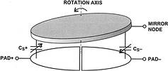
A way of accomplishing angular position measurement around one axis is to form a capacitive divider between the mirror itself and two sense electrodes beneath the structure, as shown in Figure 1. As the mirror rotates around an axis parallel to the dividing line between the two electrodes, one capacitance value increases and the other decreases. This differential capacitance can be used to measure the mirror rotation. In actual practice, of course, the electrodes are designed to sense multiple axes of rotation (see Figure 4).
A simplified version of a circuit to measure the differential capacitance is shown in Figure 2. Opposing voltage pulses are applied to each of the sense electrodes, and any differential capacitance will result in excess positive or negative charge on the mirror node itself. This charge is converted into a voltage by an on-chip amplifier. The voltage can provide a quantitative measurement of the mirror's angular position if the capacitive relationship is known.
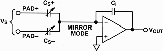
By integrating amplifier circuitry on the chip, much greater position-measurement precision is possible than can be provided with off-chip detection. The principal reason is that parasitic capacitances and cross-coupling paths associated with bond wires can easily mask the tiny positional capacitances being measured. The much smaller parasitic capacitances associated with on-chip interconnections result in a dramatic increase in signal integrity.
Fabrication
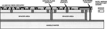
Mirrors and position sense circuitry as described above have been successfully fabricated and tested at Analog Devices. Figure 3 shows a cross-section illustrating the proprietary optical iMEMS process used to manufacture these mirrors. A 3-layer process - using silicon-on-insulator (SOI) bonding - is used to fabricate a mirror, a silicon sacrificial layer, and a circuit device layer-all on the same substrate. These components combine to allow fine-featured MEMS structures and precision high- and low-voltage BiCMOS circuitry, to coexist on the same substrate, making the capacitive mirror sensing feasible.
A scanning-electron-microscope (SEM) image of a fabricated mirror array is shown in Figure 4. This picture shows the 2-axis mirror, the position sense electronics (at bottom), and the gap underneath the mirror, which allows it to rotate. As shown, it is rotated about the 'Y' axis. Although not shown here, multiple mirrors can be fabricated on the same substrate, allowing for both high-port-count designs and the economies of scale typical of Analog Devices micromachined products.
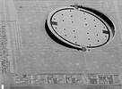
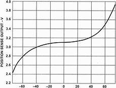
Figure 5 shows the relationship between the applied drive voltage and the output of the position-sense interface. A negative input voltage in this context refers to a voltage applied to the negative drive electrode. The classic V x |V| square-law behaviour, typical of electrostatically-driven structures, can easily be observed in the data.
Conclusions
The Analog Devices Micromachined Product Division has developed the first mirrors with on-chip capacitive position sensing. This technology promises products employing all-optical switches with improved insertion loss performance and capable of high-port-counts. These developments are the first steps toward greatly reducing the assembly costs of all-optical switches.
Information from Parsec. For more information contact the company on 012 349 2282.
*Acknowledgement
This project was a team effort at Analog Devices. The article is based on a paper submitted by the team and accepted for presentation at the European Conference on Optical Communication (ECOC). Members of the team, in addition to Trey Roessig, were Ara Arakelian, Tim Brosnihan, Bill Clark, David Han, Michael Judy, Thor Juneau, Mark Lemkin, Steve Sherman, and Jeff Swift.


© Technews Publishing (Pty) Ltd | All Rights Reserved
 printer friendly version