


Ref: z2615195m
In addition to its leadership in silicon memory technology, Intel has pioneered package technology, particularly for manufacturers of wireless devices and applications. Most recently Intel has offered manufacturers Intel 'stacked chip scale package' (CSP) technology, which offers a remarkably small form factor along with reliability, performance, and flexibility to support upgrades and feature enhancements.
Overview
For manufacturers of advanced wireless devices and applications, Intel is known for providing a winning solution of leading-edge silicon technology paired with the latest in package technology. Much has been written about the Intel Flash memory silicon technology, particularly its advanced lithography process and memory combinations. But less is known about the company's small form-factor package technology, which provides device manufacturers optimised memory capacity in a minimal space.
In 1996, the wireless industry was transformed by the invention of chip scale package (CSP) technology. The first Intel CSP product, the µBGA CSP, was significant in that its size was similar to that of the die. In the past, packaging was considerably larger than the die, but the µBGA CSP changed this, measuring roughly 70% smaller than the previous thin small outline package (TSOP) technology. By bringing a smaller form factor to the market, the µBGA CSP enabled an entirely new class of mobile phones-smaller, lighter-weight, thinner, and with significantly more features than their predecessors. Today, CSP products are used in most mobile phones worldwide.
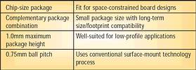
Addressing size/footprint compatibility
In 2000, Intel introduced the very-thin-profile, fine-pitch ball grid array (VF BGA) package, which addressed the need of some manufacturers to maintain the same footprint on a PCB while enjoying the advantages of next-generation silicon process lithography. Because of the rapid migration to smaller and smaller fab processes, the low-density memory die was no longer able to fit in the same CSP across densities and processes. The VF BGA package provided a solution to this dilemma by enabling the ball signals and locations to remain the same even as the die grew smaller. This package gives manufacturers long-term size/footprint compatibility along with the very thin-profile 1,0 mm package height and 0,75 mm ball pitch/spacing available earlier in the µBGA package.
Intel also addresses the needs of manufacturers by using common footprints across product lines and densities and working to ensure that all footprints conform to JEDEC standards. The VF BGA and µBGA packages are the industry's smallest single-die packages, which makes them particularly well-suited to applications where size and cost are the main considerations. In short, the VF BGA and µBGA packages enable manufacturers to control costs by keeping the same footprint on a PCB while also taking advantage of next-generation silicon lithography.
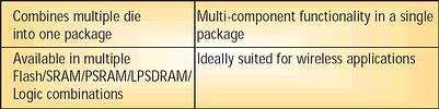
For applications where size is a critical factor and multiple-die packages are required, Intel offers the stacked-CSP, which provides a high level of integration in a small footprint. To take one example, stacked-CSP is ideal for applications requiring integrated Intel‚ Flash memory and SRAM, because it places both of the die in a single package. This approach provides continued size minimization by reducing a component from the PCB. This is particularly important for manufacturers seeking to add features and functionality while keeping their products as small as possible. (See Figure 1.)
Stacked-CSP leadership delivers choice, flexibility
Intel leads the industry in stacked-CSP technology, having manufactured and shipped more than 100 million stacked-CSP product units since 1998.This breadth of experience helps Intel to provide wireless-device manufacturers the flexibility to easily upgrade their designs to higher densities, performance, and functionality while meeting stringent requirements in size, cost, and ease of use. Today, Intel continues to lead the industry in advanced stacked-package technology providing smaller stacked-CSP products with multiple Flash devices and RAM technology combinations.
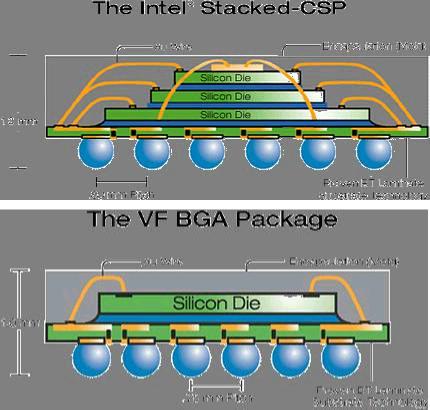
For example, advanced stacked-CSP packages allow for up to five stacked die and package heights as little as 1,0 mm. Intel's latest offering, the folded stacked-CSP, allows for even more flexibility in stacking silicon technologies, such as RAM in various sizes, low-power SDRAM, and logic; and Flash memory densities ranging from 16 Mbit to 256 Mbit and, in the future, with even lower-profile package heights.
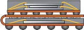
Intel's other stacked-CSP innovation is known as package-to-package stacking. Package-to-package technology allows for two or more fully tested individual packages or modules to be stacked one on top of the other in the application. This is an exciting technology for two reasons: First, it allows tremendous flexibility in stacking various types of silicon in various process steps. Second, it helps to lower the cost of the solution should any of the die require special testing or burn-in or be susceptible to yield issues after packaging.
For higher-density storage requirements, Intel is also leading the market by stacking the industry's highest-density Flash memory products, such as the Intel StrataFlash memory, with the manufacturer's choice of RAM in a single package. This high-density, small-package combination enables manufacturers to design compelling applications without concern that the larger memory requirement might consume limited board space. At the same time, Intel avoids hyperstacked package architectures in favour of proven solutions, following the philosophy that simpler is usually smaller, more reliable, and more cost-effective.
Moreover, Intel offers more than just the highest-performance silicon-process technology in advanced stacked packaging. Intel software, tools, and support provide a complete solution for application and device designers and manufacturers seeking to reduce development costs and deliver products to market that much sooner. One example of Intel's commitment to ease of use is its signal access tool, which enables a customer to gain access to pins located underneath the BGA package.
Another example is the Intel Flash Memory Chip Scale Package User's Guide. This document provides PCB design guidelines, SMT manufacturing tips, and other information essential for manufacturers and designers. For more information on these and more than 700 other tools for all stages of the product development cycle please visit the Intel Flash Memory Tools Web site at http://developer.intel.com/design/flash/tools and the Intel Flash Memory Packaging Technology Web site at http://developer.intel.com/design/flash/packtech/index.htm.
Summary
Intel's latest offerings in stacked chip scale package technology continue the tradition of Intel leadership in silicon technology by supporting manufacturers in their endeavour to build a small, reliable, and feature-packed solution for their wireless customers. Your local Intel product representative can give more information on how Intel's advanced package solutions can benefit your next wireless design.
For more information contact Memec SA, Steve Schoeman, 021 674 4103, [email protected]


© Technews Publishing (Pty) Ltd | All Rights Reserved
 printer friendly version