


Microfocus X-ray inspection is a well established standard inspection method for hidden solder joints based on standard lead-tin alloys of area array packages such as BGA, CSP and Flip Chip. Due to increasing reliability requirements, it is also applied to the traditional THT and SMT solder joints, since it reveals internal voids and visualises optically obstructed solder meniscuses. Hitherto, the solder joints could be easily displayed at excellent contrast due to X-ray absorption of lead which is relatively high compared to that of PCB and component materials such as copper and epoxy.
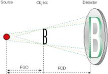
The suitability of X-ray systems for the inspection of lead-free interconnections should be considered in light of the physical fundamentals of X-ray imaging. In microfocus X-ray systems the specimen is penetrated by a coneshaped X-ray beam which generates a magnified X-ray shadow image on the detector (presently an image intensifier, in most cases). The achievable resolution or image sharpness is mainly determined by the focal spot size of the X-ray tube which is typically in the range of a few microns but can amount to significantly less than 1 micron for novel nanofocus tubes. The magnification is given by the beam's geometry (Figure 1).
Apart from magnification and contrast, the detectability of distinct object features depends on the contrast in the X-ray image caused by these features. Contrast is caused by different X-ray absorption of the different objects. Those differences in absorption can be due to variations in thickness or in material. As a rule of thumb for the image intensifier, we may assume that the absorption difference must amount to at least 2% to be clearly detected.
The physics of X-ray absorption
Physically, X-ray absorption is ruled by an exponential law:
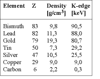
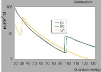
Where I/IO is the ratio of the intensity of the X-ray beam before and after passing through the specimen. The material's influence is described by the mass absorption coefficient µ/ρ which also depends on the energy of the radiation quanta. [ρ] stands for the density of the material of thickness x. Furthermore, in the X-ray energy range of 30 to 160 keV which is normally used in microfocus X-ray inspection, the mass absorption coefficient µ/ρ strongly depends on the atomic number Z (approximately it increases proportionally with Z3). In Table 1, Z is listed for some materials which might be used in lead-free interconnections.
Lead-free solder joints
Presently, most lead-free solder alloys consist mainly of bismuth or - much more frequently - tin, as in eg, SnCuAg. For bismuth (Z=83) an X-ray absorption comparable to lead solders (PbSn) can be expected whereas for tin solders (Z=50), a much lower absorption and, hence, a remarkably poorer contrast might be feared. However, inspection practice shows that for example SnCuAg solder joints yield nearly the same contrast as PbSn solder joints (Figure 2).
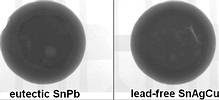
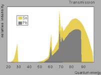
This can be understood immediately on the basis of the mass absorption coefficient (see Figure 3). The K-absorption edge of tin is located as low as 30 keV so that its mass absorption coefficient is even higher than that of lead or lead-tin alloys up to the K-absorption edge of lead at 88 keV. A numerical simulation (Figure 4) shows that tin solder joints can be expected to transmit a little more radiation within the image intensifier's most sensitive energy range (30 to 100 keV). And indeed, the lead-free solder joint in Figure 2 on the right appears slightly brighter than the PbSn solder joint on the left.
Practical experiences
In inspection servicing, all test criteria for solder joint integrity and all signatures of the soldering process turned out to be clearly visible and valid for lead-free solder joints. Moreover, there are no restrictions concerning the automatic inspection and evaluation of lead-free BGA and CSP solder joints. This has been proven, in particular, during a screening within an investigation of void development in lead-free PBGA solder joints (Sn96Ag4 and Sn95,5Ag4Cu0,5). Mixed lots of lead-free and lead-tin solder joints could be inspected by the auto-setup BGA evaluation software without changing thresholds or X-ray parameters.
Other lead-free interconnections
First X-ray inspections on adhesive interconnections in Flip Chips have been successfully performed. Here, stud-bumped Flip Chips were attached to the lands on a PCB by isotropic silver-filled glue. The interconnections could be securely inspected for mis-registration, adhesive distribution, short circuits etc. However, to evaluate those interconnections professionally, more experience and standardisation of criteria may still be necessary.
For interconnection media of very low contrast novel digital detectors have been developed which typically provide a contrast resolution four times better than that of the image intensifier.
The future of X-ray inspection
Dispelling widespread doubts, lead-free and, in particular, tin-based solder joints can be inspected without any problems provided that the X-ray system is of appropriate performance. Up to now, the appearance, at least, of the Sn based solder joints is quite similar to that of the PbSn solder joints and systematic deviations in thickness or shape have not yet been found.
To find X-ray inspection solutions for alternative interconnections such as adhesive bonding, the capabilities of X-ray inspection should be evaluated experimentally using the latest in X-ray equipment. Good results could be achieved for eg, with silver-filled adhesives.
| Tel: | +27 11 609 1244 |
| Email: | [email protected] |
| www: | www.zetech.co.za |
| Articles: | More information and articles about ZETECH ONE |


© Technews Publishing (Pty) Ltd | All Rights Reserved
 printer friendly version