Solder inspection system offers high magnification for accurate inspections
25 February 2004
Manufacturing / Production Technology, Hardware & Services
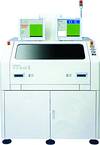
Incorporating the versatile Windows 2000 interface, Omron's VT-WIN II PCB solder inspection system can be used either in-line or off-line, for rapid, accurate identification of a variety of circuit board assembly defects. A zoom lens allows multiple magnifications down to 10 microns per pixel. According to the company, the VT-WIN II's magnification is the highest in the industry, allowing it to accurately inspect 0201 components. In addition, with its high speed digital camera and high speed motion control, it is also one of the fastest inspection systems around - and twice as fast as the previous VT-WIN model.
Figure 1. The VT-WIN II offers advances in solder inspection, component fault detection and process speed that gives manufacturers a competitive edge in productivity, waste reduction and quality control
Major improvements with VT-WIN II are: angled-view inspection to detect lifted leads on gullwing devices and heel fillets on SOJ and PLCC devices; industry-leading algorithms to accurately inspect lead-free solder; four times the inspection area and twice the speed; automatic colour extraction tool and other teaching aid functions dramatically reduce setup time.
First introduced in 1996, the original VT-WIN revolutionised in-line PCB inspection with a patented Colour Highlight System and colour image processing. Omron's VT-WIN II handles a variety of PCB styles, increasing production flexibility. The Colour Highlight System enables instant, consistently accurate recognition of solder quality, wettability and correct component placement. Accuracy is also enhanced through the system's position self-adjustment function. This function enables the system to automatically adjust solder land size inspection area allowing simplified programming of varying land sizes.
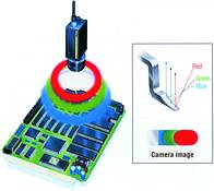
Figure 2. Omron’s Colour Highlight System projects red, green and blue light onto the PCB at different angles. The camera captures these reflected colours, producing a two-dimensional image that conveys three-dimensional information that allows the VT-WIN II to detect minute flaws that would commonly be missed
The Colour Highlight System uses a multicolour LED light source to project red, green and blue light onto the PCB at different angles. The camera captures these colours as they reflect off the board's surface, producing a two-dimensional image that conveys three-dimensional information. This image allows the VT-WIN II to detect minute flaws that would ordinarily be missed. Compared to gray-scale inspection methods, where solder fillet image settings are defined with numerical values for brightness and contrast, this process is significantly easier, reduces errors due to misinterpretation of data or colours, and ultimately reduces start-up time.
Another aspect of the VT-WIN II's functionality is its optical character recognition (OCR) capability, in which it distinguishes correct component values, thus preventing incorrect assemblies. The system also has advanced algorithms that enable proper inspection of leading technology processes such as lead-free solder. The software, which is programmed via CAD placement data, incorporates intelligent algorithms to reduce operator programming time. Omron's graphical user interface allows parameter settings to be defined via a 'point-and-click method' rather than requiring numerical values to be entered.
For more information contact Hawker Richardson, 011 792 2766.
Further reading:
World-first 016008 mm component placement
Manufacturing / Production Technology, Hardware & Services
Fuji has achieved the world’s first placement of 016008 mm (0,16 x 0,08 mm or 006 x 003 inches) size components on printed circuit boards with its SMT pick and place machine, NXTR.
Read more...
Lifecycle and obsolescence: Protecting electronics through process
Production Logix
Manufacturing / Production Technology, Hardware & Services
At Production Logix, we believe longevity is not accidental. It is engineered through early visibility, structured response, and disciplined execution, in partnership with our OEM customers.
Read more...
Maximising squeegee quality and durability
Testerion
Manufacturing / Production Technology, Hardware & Services
Transition Automation has announced two new product advancements designed to improve SMT printing performance and extend squeegee life: laser-enhanced Permalex bonding and integrated edge protectors.
Read more...
NeoDen ND2 PCB screen printer
ZETECH ONE
Manufacturing / Production Technology, Hardware & Services
The NeoDen ND2 PCB screen printing machine is a fully automatic stencil printer designed to deliver precise and consistent solder paste application in modern SMT production environments.
Read more...
Understanding the BGA rework process
Techmet
Manufacturing / Production Technology, Hardware & Services
BGA rework is a highly technical process that involves removing the faulty component, preparing the circuit board, and installing a new or repaired device, while maintaining the integrity of the printed circuit board.
Read more...
Flexible three-process reflow soldering system
Truth Electronic Manufacturing
Manufacturing / Production Technology, Hardware & Services
By combining multiple soldering technologies within a single system, the Vision TripleX system enables manufacturers to adapt easily to different assembly requirements, board designs, and production volumes.
Read more...
Inline vapour phase soldering for high-volume production
MyKay Tronics
Manufacturing / Production Technology, Hardware & Services
The VP2200-100 vacuum inline vapour phase soldering system from ASSCON is designed for fully automated, high-volume electronics manufacturing where process consistency and solder joint quality are critical.
Read more...
Global electronics solutions since 1964
IMP Electronics Solutions
Manufacturing / Production Technology, Hardware & Services
Over more than six decades, IMP Electronics Solutions has built a reputation for technical expertise, reliable supply chains, and strong partnerships with both customers and manufacturing partners.
Read more...
Driving excellence in electronics manufacturing
Jemstech
Editor's Choice Manufacturing / Production Technology, Hardware & Services
Jemstech’s reputation for disciplined execution and client-focused service has earned it strong loyalty from companies operating in demanding industries.
Read more...
When do you need Nitrogen in reflow?
Truth Electronic Manufacturing
Manufacturing / Production Technology, Hardware & Services
Nitrogen in reflow soldering is often seen as a performance enhancer, offering improved wetting, shinier joints, and fewer defects. But it is not always necessary.
Read more...


 printer friendly version